
下载
ADS58C28
www.ti.com
SBAS509B –JUNE 2010–REVISED OCTOBER 2010
Dual Channel IF Receiver with SNRBoost
3G
Check for Samples: ADS58C28
1
FEATURES
DESCRIPTION
23
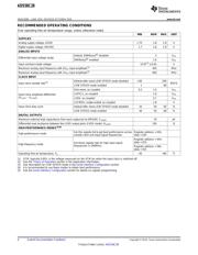
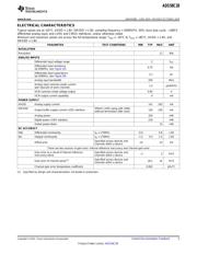
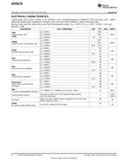
• Maximum Sample Rate: 200MSPS
The ADS58C28 is a dual-channel, 11-bit
analog-to-digital converter (ADC) with sampling rates
• High Dynamic Performance:
up to 200MSPS. The device uses innovative design
– 83dBc SFDR at 140MHz
techniques to achieve high dynamic performance,
– 72.5dBFS SNR with 60MHz BW Using
while consuming extremely low power at 1.8V supply.
SNRBoost
3G
Technology
This architecture makes it well-suited for multi-carrier,
wide bandwidth communications applications.
• SNRBoost
3G
Highlights:
– Supports Wide Bandwidth (up to 60MHz)
The ADS58C28 uses third-generation SNRBoost
3G
technology to overcome SNR limitation as a result of
– Programmable Bandwidths:
quantization noise (for bandwidths less than Nyquist,
20MHz, 30MHz, and 40MHz
f
S
/2). Enhancements in the SNRBoost
3G
technology
– Flat Noise Floor within the Band
allow support for SNR improvements over wide
– Independent SNRBoost
3G
Coefficients for
bandwidths (up to 60MHz). In addition, separate
Both Channels
SNRBoost
3G
coefficients can also be programmed for
each channel.
• Output Interface:
The device has a digital gain function that can be
– Double Data Rate (DDR) LVDS with
used to improve SFDR performance at lower
Programmable Swing and Strength:
full-scale input ranges. It includes a dc offset
– Standard Swing: 350mV
correction loop that can be used to cancel the ADC
– Low Swing: 200mV
offset. The digital outputs of all channels are output
as double data rate (DDR) low-voltage differential
– Default Strength: 100Ω termination
signaling (LVDS) together with an LVDS clock output.
– 2x Strength: 50Ω termination
The low data rate of this interface (400MBPS at
– Compatible with GC6016
200MSPS sample rate) makes it possible to use
– 1.8V Parallel CMOS Interface Also
low-cost field-programmable gate array
(FPGA)-based receivers. The strength of the LVDS
Supported
output buffers can be increased to support 50Ω
• Ultralow Power with Single 1.8V Supply:
differential termination. This increase allows the
– 470mW Total Power
output clock signal to be connected to two separate
– 710mW Total Power (200MSPS) with receiver chips with an effective 50Ω termination (such
as the two clock ports of the GC5330). The same
SNRBoost
3G
on Both Channels
digital output pins can also be configured as a parallel
• Programmable Gain up to 6dB for
1.8V CMOS interface.
SNR/SFDR Trade-off
The device includes internal references while the
• DC Offset Correction
traditional reference pins and associated decoupling
• Supports Low Input Clock Amplitude
capacitors have been eliminated. The ADS58C28 is
• Package: QFN-64 (9mm × 9mm)
specified over the industrial temperature range
(–40°C to +85°C).
1
Please be aware that an important notice concerning availability, standard warranty, and use in critical applications of Texas
Instruments semiconductor products and disclaimers thereto appears at the end of this data sheet.
2PowerPAD is a trademark of Texas Instruments Incorporated.
3All other trademarks are the property of their respective owners.
PRODUCTION DATA information is current as of publication date.
Copyright © 2010, Texas Instruments Incorporated
Products conform to specifications per the terms of the Texas
Instruments standard warranty. Production processing does not
necessarily include testing of all parameters.