

下载

© Semiconductor Components Industries, LLC, 2010
February, 2010 − Rev. 0
1 Publication Order Number:
ADP3208D/D
ADP3208C
7-Bit, Programmable,
Dual-Phase, Mobile, CPU,
Synchronous Buck
Controller
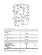
The ADP3208C is a highly efficient, multiphase, synchronous buck
switching regulator controller. With its integrated drivers, the
ADP3208C is optimized for converting the notebook battery voltage
into the core supply voltage required by high performance Intel
processors. An internal 7−bit DAC is used to read a VID code directly
from the processor and to set the CPU core voltage to a value within
the range of 0.3 V to 1.5 V. The phase relationship of the output signals
ensures interleaved 2−phase operation.
The ADP3208C uses a multi−mode architecture run at a
programmable switching frequency and optimized for efficiency
depending on the output current requirement. The ADP3208C
switches between single− and dual−phase operation to maximize
efficiency with all load conditions. The chip includes a programmable
load line slope function to adjust the output voltage as a function of the
load current so that the core voltage is always optimally positioned for
a load transient. The ADP3208C also provides accurate and reliable
short−circuit protection, adjustable current limiting, and a delayed
power−good output. The IC supports On−The−Fly (OTF) output
voltage changes requested by the CPU.
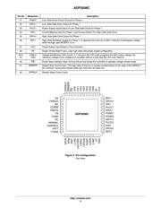
The ADP3208C is specified over the extended commercial
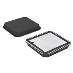
temperature range of −10°C to 100°C and is available in a 48−lead
LFCSP.
Features
• Single−Chip Solution
• Fully Compatible with the Intel
®
IMVP−6+t
Specifications
• Integrated MOSFET Drivers
• Input Voltage Range of 3.3 V to 22 V
• Selectable 1− or 2−Phase Operation with Up to 1 MHz
per Phase Switching Frequency
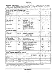
• Guaranteed ±8 mV Worst−Case Differentially Sensed
Core Voltage Error Overtemperature
• Automatic Power−Saving Mode Maximizes Efficiency
with Light Load During Deeper Sleep Operation
• Soft Transient Control Reduces Inrush Current and
Audio Noise
• Active Current Balancing Between Output Phases
• Independent Current Limit and Load Line Setting
Inputs for Additional Design Flexibility
• Built−In Power−Good Blanking Supports Voltage
Identification (VID) OTF Transients
• 7−Bit, Digitally Programmable DAC with 0.3 V to
1.5 V Output
• Short−Circuit Protection with Latchoff Delay
• Clock Enable Output Delays the CPU Clock Until the
Core Voltage is Stable
• Output Load Current Monitor
• This is a Pb−Free Device
Applications
• Notebook Power Supplies for Next Generation
Intel
®
Processors
MARKING DIAGRAM
http://onsemi.com
See detailed ordering and shipping information in the package
dimensions section on page 36 of this data sheet.
ORDERING INFORMATION
LFCSP48
CASE 932AD
ADP3208C
AWLYYWWG
A = Assembly Location
WL = Wafer Lot
YYWW = Date Code
G = Pb−Free Package
页面指南