
下载
Programmable Low Power Gyroscope
Evaluation Board
Preliminary Technical Data
ADIS1625x/PCB
Rev. PrE
Evaluation boards are only intended for device evaluation and not for production purposes.
Evaluation boards as supplied “as is” and without warranties of any kind, express, implied, or
statutory including, but not limited to, any implied warranty of merchantability or fitness for a
particular purpose. No license is granted by implication or otherwise under any patents or other
intellectual property by application or use of evaluation boards. Information furnished by Analog
Devices is believed to be accurate and reliable. However, no responsibility is assumed by Analog
Devices for its use, nor for any infringements of patents or other rights of third parties that may result
from its use. Analog Devices reserves the right to change devices or specifications at any time
without notice. Trademarks and registered trademarks are the property of their respective owners.
Evaluation boards are not authorized to be used in life support devices or systems.
One Technology Way, P.O. Box 9106, Norwood, MA 02062-9106, U.S.A.
Tel: 781.329.4700 www.analog.com
Fax: 781.461.3113 ©2007 Analog Devices, Inc. All rights reserved.
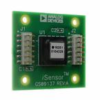
GENERAL DESCRIPTION
The ADIS16250/PCB, ADIS16251/PCB, and ADIS16255/PCB
are simple evaluation boards that provide convenient access to
the ADIS16250, ADIS16251, ADIS16255 using a standard
2 mm, 2 × 6, connector interface. These connectors can be
accessed using a variety of cable options, including standard
1 mm ribbon cables. The ADIS1625x/PCB is designed to be
evaluated in an existing digital platform (such as MCU, DSP,
FPGA, PLD) or as part of the ADISEVAL system. Four
mounting holes (sized for 2-56 or 2 mm screws) have been
provided to secure the board during evaluation.
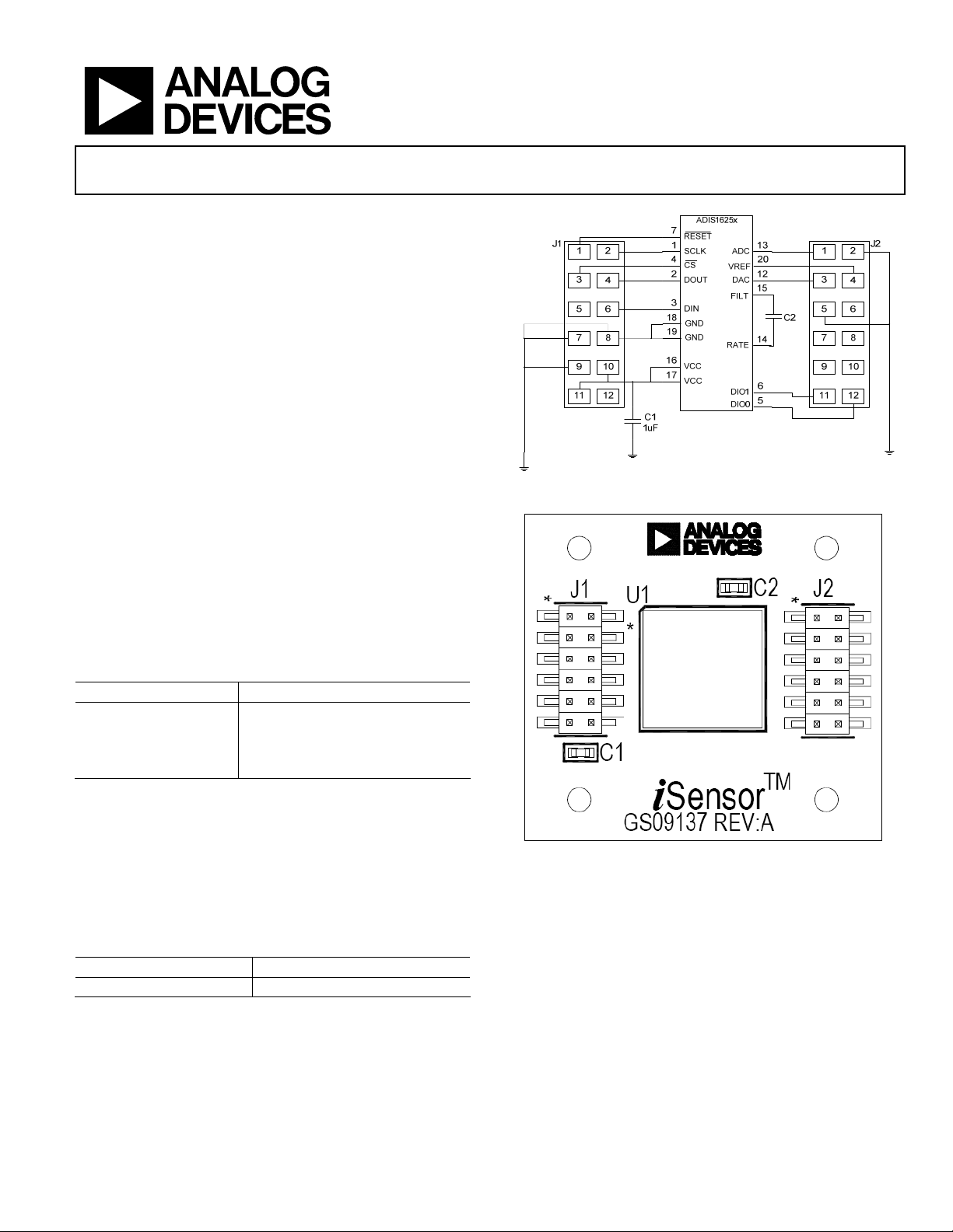
CIRCUIT DESCRIPTION
The schematic, layout, and parts list for the ADIS1625x/PCB
can be found in
Figure 1, Figure 2, and Table 1.
The ADIS1625x’s digitized outputs can be accessed using the
4-wire serial port interface (SPI) signals on J1: SCLK, CS, DOUT,
and DIN. For specific information on using the ADIS1625x SPI
interface, refer to the
ADIS16250 data sheet. Auxiliary functions,
such as the 12-bit ADC input, can be accessed using J2. C1
provides additional power supply filtering but is generally not
required. C2 provides pads for installing a capacitor to reduce
the ADIS1625x’s bandwidth.
Table 1. ADIS1625x/PCB Parts List
Reference Designator Part Description
U1 ADIS1625xACCZ
1
J1, J2 12-pin, dual row, 2 mm connector
C1 Power supply filtering, not installed
C2 Bandwidth adjust, not installed
1
x = 0, 1, or 5.
SPECIAL NOTES ON HANDLING
Note that the ADIS1625x/PCB is not reverse-polarity protected.
Reversing the power supply or applying inappropriate voltages
(that is, voltages outside the Absolute Maximum Ratings in the
ADIS16250 data sheet) to any pin may damage the ADIS1625x/PCB.
Table 2. Power Supply Levels
Parameter Range
V
CC
4.75 V to 5.25 V
Figure 1. ADIS1625x/PCB Schematic
Figure 2. ADIS1625x/PCB Layout (Top View)