


下载
AN-1217
APPLICATION NOTE
One Technology Way • P. O. Box 9106 • Norwood, MA 02062-9106, U.S.A. • Tel: 781.329.4700 • Fax: 781.461.3113 • www.analog.com
Clock Distribution Circuit with Pin-Programmable Output Frequency, Output Logic
Levels, and Fanout
Rev. B | Page 1 of 4
EVALUATION AND DESIGN SUPPORT
Circuit Evaluation Boards
AD9552 Evaluation Board (AD9552-PCBZ)
ADCLK854 Evaluation Board (ADCLK854-PCBZ)
Design and Integration Files
Schematics, Layout Files, Bill of Materials
Software
CIRCUIT FUNCTION AND BENEFITS
The AD9552 oscillator frequency upconverter and ADCLK854
LVDS/CMOS clock fanout buffer together create a flexible clock
distribution solution that is pin-programmable. The AD9552 is
equipped with an SPI port to program the device. This interface
enables a wide output frequency range up to 900 MHz. However, it
is also pin-programmable which simplifies use in many designs
that do not require software programmability.
In the pin-programmable mode, there are up to 64 standard output
frequencies available, based on the input frequency selection. The
AD9552, therefore, functions like a frequency pin-programmable
VCXO. The AD9552 is also equipped to operate from a crystal
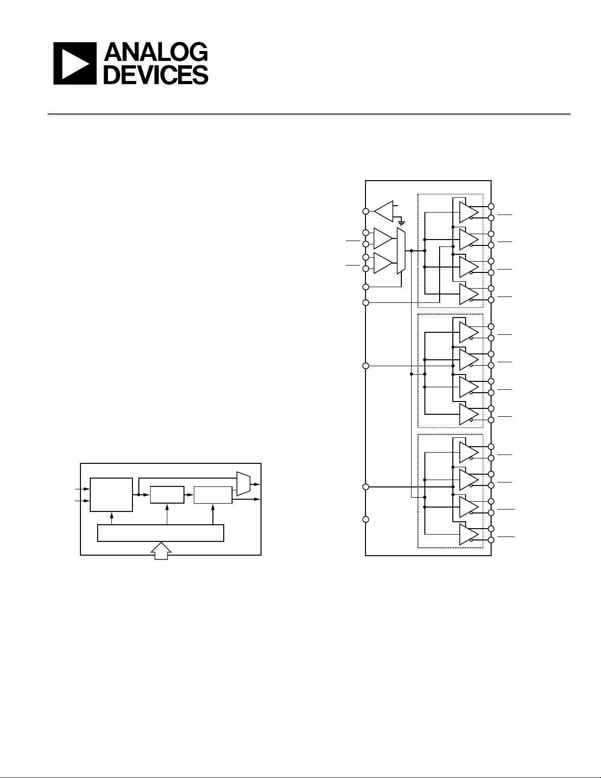
resonator at the input for additional flexibility. A simplified block
diagram of the AD9552 is shown in Figure 1, and a simplified
block diagram of the ADCLK854 is shown in Figure 2.
AD9552
INPUT
FREQUENCY
SOURCE
SELECTOR
PLL
REF
XTAL
OUT2
OUT1
OUTPUT
CIRCUITRY
08978-001
PIN-DEFINED AND SERIAL PROGRAMMING
Figure 1. Simplified Block Diagram of AD9552 Oscillator Frequency
Upconverter
OUT0 (OUT0A)
OUT0 (OUT0B)
OUT1 (OUT1A)
OUT1 (OUT1B)
OUT2 (OUT2A)
OUT2 (OUT2B)
OUT3 (OUT3A)
OUT3 (OUT3B)
LVDS/
CMOS
OUT4 (OUT4A)
OUT4 (OUT4B)
OUT5 (OUT5A)
OUT5 (OUT5B)
OUT6 (OUT6A)
OUT6 (OUT6B)
OUT7 (OUT7A)
OUT7 (OUT7B)
LVDS/
CMOS
OUT8 (OUT8A)
OUT8 (OUT8B)
OUT9 (OUT9A)
OUT9 (OUT9B)
OUT10 (OUT10A)
OUT10 (OUT10B)
OUT11 (OUT11A)
OUT11 (OUT11B)
LVDS/
CMOS
CTRL_C
CTRL_B
CTRL_A
IN_SEL
SLEEP
CLK1
CLK1
CLK0
CLK0
ADCLK854
V
REF
V
S
/2
08978-002
Figure 2. Simplified Block Diagram of ADCLK854 Clock Fanout Buffer
The ADCLK854 is a clock fanout buffer and is pin-programmable
for both LVDS and 1.8 V CMOS outputs. The ADCLK854 has
up to 12 LVDS outputs, 24 CMOS outputs, or combinations of
both. The ADCLK854 could be replaced with several other clock
fanout clock buffers available from Analog Devices with fewer
outputs and/or different output logic choices.