


下载

Low Power, 8.5 mW, 2.3 V to 5.5 V,
Programmable Waveform Generator
Data Sheet
AD9837
Rev. A Document Feedback
Information furnished by Analog Devices is believed to be accurate and reliable. However, no
responsibility is assumed by Analog Devices for its use, nor for any infringements of patents or other
rights of third parties that may result from its use. Specifications subject to change without notice. No
license is granted by implication or otherwise under any patent or patent rights of Analog Devices.
Trademarks and registered trademarks are the property of their respective owners.
One Technology Way, P.O. Box 9106, Norwood, MA 02062-9106, U.S.A.
Tel: 781.329.4700 ©2011–2012 Analog Devices, Inc. All rights reserved.
Technical Support www.analog.com
FEATURES
Digitally programmable frequency and phase
8.5 mW power consumption at 2.3 V
MCLK speed: 16 MHz (B grade), 5 MHz (A grade)
28-bit resolution: 0.06 Hz at 16 MHz reference clock
Sinusoidal, triangular, and square wave outputs
2.3 V to 5.5 V power supply
3-wire SPI interface
Extended temperature range: −40°C to +125°C
Power-down option
10-lead LFCSP
APPLICATIONS
Frequency stimulus/waveform generation
Liquid and gas flow measurement
Sensory applications: proximity, motion,
and defect detection
Line loss/attenuation
Test and medical equipment
Sweep/clock generators
Time domain reflectometry (TDR) applications
GENERAL DESCRIPTION
The AD9837 is a low power, programmable waveform generator
capable of producing sine, triangular, and square wave outputs.
Waveform generation is required in various types of sensing,
actuation, and time domain reflectometry (TDR) applications.
The output frequency and phase are software programmable,
allowing easy tuning. The frequency registers are 28 bits wide:
with a 16 MHz clock rate, resolution of 0.06 Hz can be achieved;
with a 5 MHz clock rate, the AD9837 can be tuned to 0.02 Hz
resolution.
The AD9837 is written to via a 3-wire serial interface. This serial
interface operates at clock rates up to 40 MHz and is compatible
with DSP and microcontroller standards. The device operates
with a power supply from 2.3 V to 5.5 V.
The AD9837 has a power-down (sleep) function. Sections of the
device that are not being used can be powered down to minimize
the current consumption of the part. For example, the DAC can
be powered down when a clock output is being generated.
The AD9837 is available in a 10-lead LFCSP_WD package.
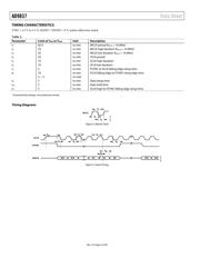
FUNCTIONAL BLOCK DIAGRAM
SERIAL INTERFACE
AND
CONTROL LOGIC
SCLK SDATAFSYNC
16-BIT CONTROL REGISTER
12-BIT PHASE1 REG
12-BIT PHASE0 REG
MUX
SIN
ROM
10-BIT DAC
MUX
12
ON-BOARD
REFERENCE
AGND
DGND
VDD
AD9837
PHASE
ACCUMULA
TOR
(28-BIT)
REGULATOR
CAP/2.5V
2.5V
AVDD/
DVDD
MUX
DIVIDE
BY 2
MSB
MUX
FULL-SCALE
CONTR
OL
COMP
VOUT
R
200Ω
09070-001
MCLK
28-BIT FREQ1 REG
28-BIT FREQ0 REG
Figure 1.
页面指南