
下载
Circuit Note
CN-0055
Circuit Designs Using Analog Devices Products
Apply these product pairings quickly and with confidence.
For more information and/or support call 1-800-AnalogD
(1-800-262-5643) or visit www.analog.com/circuit.
Devices Connected/Referenced
AD5450/AD5451/
AD5452/AD5453
8-/10-/12-/14-Bit Multiplying
DAC
AD8065
High Performance FastFET
TM
Amplifier
Programmable Gain Element Using the AD5450/AD5451/AD5452/AD5453
Current Output DAC Family
Rev. A
“Circuits from the Lab” from Analog Devices have been designed and built by Analog Devices
engineers. Standard engineering practices have been employed in the design and construction of
each circuit, and their function and performance have been tested and verified in a lab environment
at room temperature. However, you are solely responsible for testing the circuit and determining its
suitability and applicability for your use and application. Accordingly, in no event shall Analog
Devices be liable for direct, indirect, special, incidental, consequential or punitive damages due to
any cause whatsoever connected to the use of any “Circuit from the Lab”. (Continued on last page)
One Technology Way, P.O. Box 9106, Norwood, MA 02062-9106, U.S.A.
Tel: 781.329.4700
www.analog.com
Fax: 781.461.3113 ©2009 Analog Devices, Inc. All rights reserved.
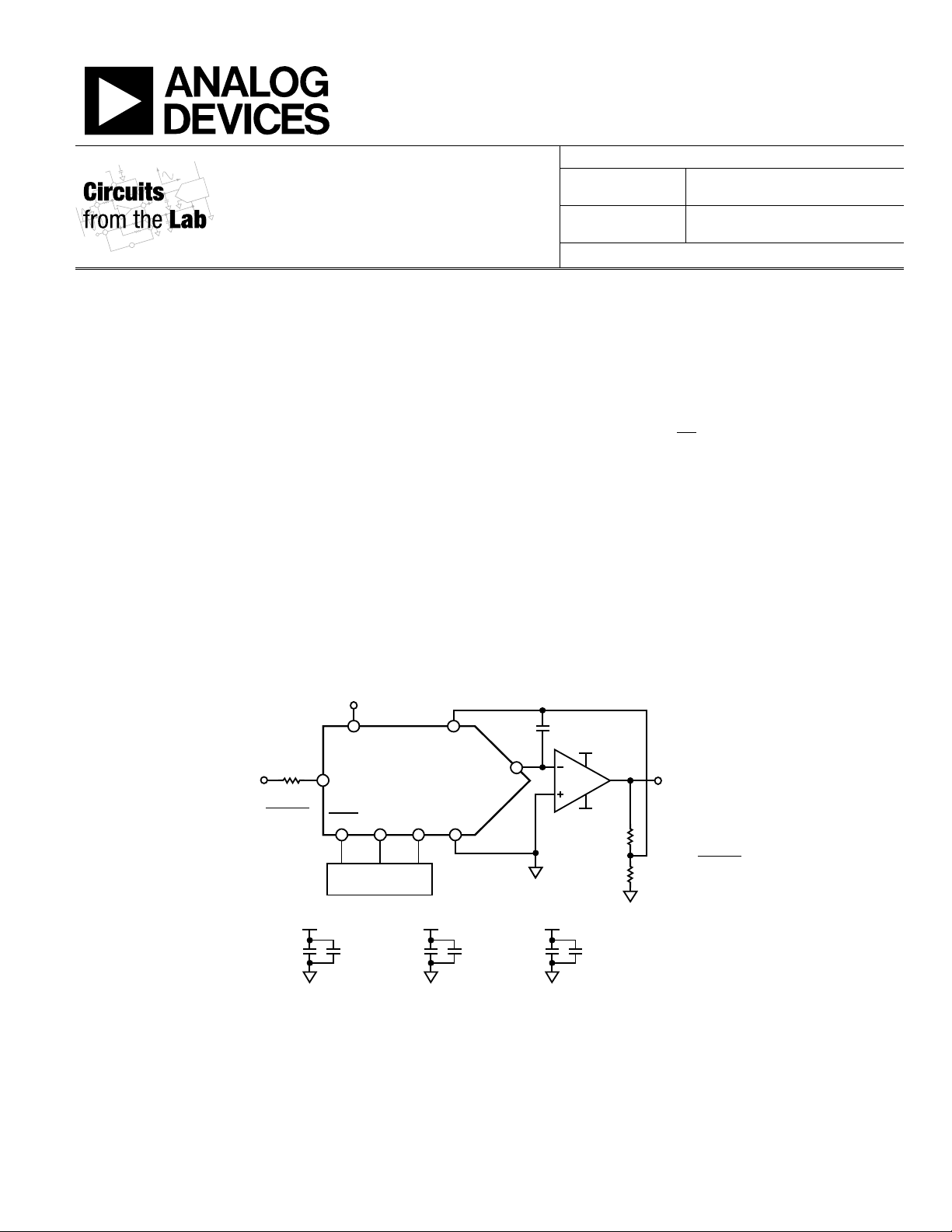
CIRCUIT FUNCTION AND BENEFITS
In applications where the DAC output voltage range is required
to be larger than the input voltage, a programmable gain circuit
can be used. This circuit provides a programmable gain
function using a multiplying DAC, the AD5450/AD5451/
AD5452/AD5453, and a fast, low offset operational amplifier,
the AD8065. The maximum gain value and the temperature
coefficient are set by external resistors, and the resolution of the
programmable gain is set by the resolution of the DAC.
CIRCUIT DESCRIPTION
The circuit shown in Figure 1 is the recommended method of
increasing the gain of the circuit. R1, R2, and R3 should all have
similar temperature coefficients, but they need not match the
temperature coefficients of the DAC. This approach is recom-
mended in circuits where gains of greater than 1 are required.
N
IN
OUT
D
VGainV
2
– ××=
(1)
where D is the digital word loaded to the DAC. D = 0 to 255
(8-bit AD5450), D = 0 to 1023 (10-bit AD5451), D = 0 to 4095
(12-bit AD5452), D = 0 to 16383 (14-bit AD5453); N is the
number of bits.
The key benefit of this circuit is its ability to overcome gain TC
errors using resistor matching. The TC of the external resistors
needs to match each other but do not need to match that of the
DAC internal ladder resistance.
08620-001
R
FB
I
OUT
1
SCLK SDIN
GND
V
IN
V
REF
SYNC
AD5450/
AD5451/
AD5452/
AD5453
V
DD
V
DD
= +5V
AGND
4.7pF
V
OUT
µCONTROLLER
AD8065
V
DD1
= +12V
V
SS
= –12V
V
DD
10µF 0.1µF
V
SS
10µF 0.1µF
V
DD1
10µF 0.1µF
R1
R2
R3
R1 =
R2 × R3
R2 + R3
GAIN =
R2 + R3
R2
Figure 1. Programmable Gain Circuit Using a Current Output DAC (Simplified Schematic: Decoupling and All Connections Not Shown)