


下载
Industrial Current Out Driver, Single-Supply,
55 V Maximum Supply, Programmable Ranges
Data Sheet
AD5749
Rev. D
Document Feedback
Information furnished by Analog Devices is believed to be accurate and reliable. However, no
responsibility is assumed by Analog Devices for its use, nor for any infringements of patents or other
rights of third parties that may result from its use. Specifications subject to change without notice. No
license is granted by implication or otherwise under any patent or patent rights of Analog Devices.
Trademarks and registered trademarks are the property of their respective owners.
One Technology Way, P.O. Box 9106, Norwood, MA 02062-9106, U.S.A.
Tel: 781.329.4700 ©2010–2018 Analog Devices, Inc. All rights reserved.
Technical Support www.analog.com
FEATURES
Current output ranges: 0 mA to 24 mA or 4 mA to 20 mA
±0.03% FSR typical total unadjusted error (TUE)
±5 ppm/°C typical output drift
2% overrange
Flexible serial digital interface
On-chip output fault detection
PEC error checking
Asynchronous CLEAR function
Power supply range
AV
DD
: 12 V (± 10%) to 55 V (maximum)
Output loop compliance to AV
DD
− 2.75 V
Temperature range: −40°C to +105°C
32-lead, 5 mm × 5 mm LFCSP package
APPLICATIONS
Process control
Actuator control
PLCs
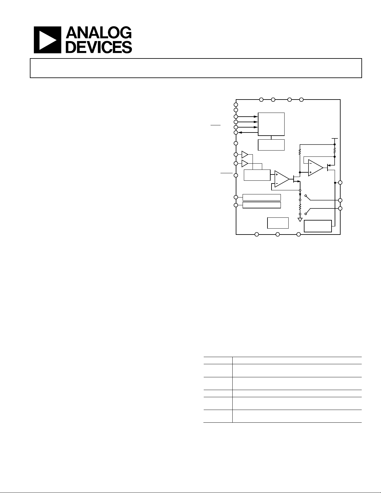
FUNCTIONAL BLOCK DIAGRAM
Figure 1.
GENERAL DESCRIPTION
The AD5749 is a single channel, low cost, precision, current output
driver with hardware or software programmable output ranges.
The software ranges are configured via an SPI-/MICROWIRE™-
compatible serial interface. The AD5749 targets applications in
PLC and industrial process control. The analog input to the
AD5749 is provided from a low voltage, single-supply digital-to-
analog converter (DAC) and is internally conditioned to provide
the desired output current/voltage range.
The output current range is programmable across two current
ranges: 0 mA to 24 mA, or 4 mA to 20 mA. Current output is
open-circuit protected and can drive inductive loads of 0.1 H.
The device is specified to operate with a power supply range
from 10.8 V to 55 V. Output loop compliance is 0 V to AV
DD
−
2.75 V.
The flexible serial interface is SPI and MICROWIRE compatible
and can be operated in 3-wire mode to minimize the digital
isolation required in isolated applications. The interface also
features an optional PEC error checking feature using CRC-8
error checking, useful in industrial environments where data
communication corruption can occur.
The device also includes a power-on reset function ensuring
that the device powers up in a known state and an asynchron-
ous CLEAR pin that sets the outputs to the low end of the
selected current range.
An HW SELECT pin is used to configure the part for hardware
or software mode on power-up.
Table 1. Related Devices
Part No. Description
AD5750
Industrial current/voltage output (I/V) driver with
programmable ranges
AD5751
Industrial I/V output driver, single-supply, 55 V maximum
supply, programmable ranges
AD5748 Industrial I/V output driver with programmable ranges
AD5410/
AD5420
Single-channel, 12-/16-bit, serial input, current source
output DAC
AD5412/
AD5422
Single-channel, 12-/16-bit, serial input, I/V output DAC
08923-001
*
DENOTES SHARED PIN. SOFTWARE MODE DENOTED BY REGULAR TEXT,
HARDWARE MODE DENOTED BY ITALIC TEXT. FOR EXAMPLE, F
OR
FAULT/TEMP PIN, IN SOFTWARE MODE, THIS PIN TAKES ON FAULT
FUNCTION. IN HARDWARE MODE, THIS PIN TAKES ON TEMP FUNCTION.
CLEAR
DVCC GND AVDD GND
CLRSEL
HW SELECT
VIN
VREF
OVERTEMP
IOUT OPEN FAULT
IOUT OPEN FAULT
RESET
R2
R
SET
AVDD
R3
AD5749
IOUT
POWER-
ON RESET
IOUT
OPEN FAULT
IOUT RANGE
SCALING
STATUS
REGISTER
INPUT SHIFT
REGISTER
AND
CONTROL
LOGIC
SCLK/OUTEN*
SDIN/R0*
SYNC/RSET*
SDO
FAULT/T EMP*
NC/IFAULT*
AD2/R1* AD1/R2* AD0/R3*
REXT1
REXT2
页面指南