


下载
32-Channel, 14-Bit DAC with Full-Scale Output
Voltage Programmable from 50 V to 200 V
Data Sheet
AD5535B
Rev. A Document Feedback
Information furnished by Analog Devices is believed to be accurate and reliable. However, no
responsibility is assumed by Analog Devices for its use, nor for any infringements of patents or other
rights of third parties that may result from its use. Specifications subject to change without notice. No
license is granted by implication or otherwise under any patent or patent rights of Analog Devices.
Trademarks and registered trademarks are the property of their respective owners.
One Technology Way, P.O. Box 9106, Norwood, MA 02062-9106, U.S.A.
Tel: 781.329.4700 ©2013 Analog Devices, Inc. All rights reserved.
Technical Support www.analog.com
FEATURES
High integration
32-channel, 14-bit denseDAC® with integrated high
voltage output amplifier
Guaranteed monotonic
Housed in 15 mm × 15 mm CSP_BGA package
Full-scale output voltage programmable from 50 V to 200 V
via reference input
550 µA drive capability
Integrated silicon diode for temperature monitoring
DSP-/microcontroller-compatible serial interface
1.2 MHz channel update rate
Asynchronous
RESET
facility
–10°C to +85°C temperature range
APPLICATIONS
Optical microelectromechanical systems (MEMS)
Optical crosspoint switches
Micropositioning applications using piezoelectric actuators
Level setting in automotive test and measurement
GENERAL DESCRIPTION
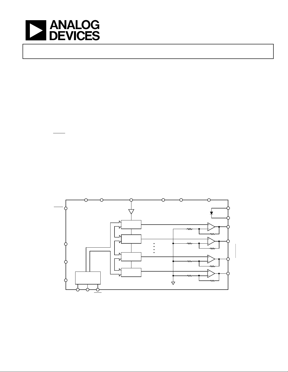
The AD5535B is a 32-channel, 14-bit denseDAC® with an on-chip
high voltage output amplifier. This device is targeted for optical
micro-electromechanical systems. The output voltage range is
programmable via the REF_IN pin. The output range is 0 V to
50 V when REF_IN = 1 V, and 0 V to 200 V when REF_IN = 4 V.
Each amplifier can source 550 µA, which is ideal for the deflection
and control of optical MEMS mirrors.
The selected digital-to-analog converter (DAC) register is written
to via the 3-wire interface. The serial interface operates at clock
rates of up to 30 MHz and is compatible with DSP and micro-
controller interface standards.
The device is operated with AV
CC
= 4.75 V to 5.25 V, DV
CC
=
2.7 V to 5.25 V, V
+
= 4.75 V to 5.25 V, and V
PP
of up to 225 V.
REF_IN is buffered internally on the AD5535B and should be
driven from a stable reference source.
FUNCTIONAL BLOCK DIAGRAM
Figure 1.
RF
R1
RF
R1
RF
R1
RF
R1
INTERFACE
CONTROL
LOGIC
DAC
DAC
DAC
DAC
DV
CC
AV
CC
SYNC
D
IN
SCLK
DGND
AGND
DAC_GND
RESET
REF_IN
V
PP
PGND
V
+
14-BIT BUS
ANODE
CATHODE
V
OUT
0
V
OUT
1
V
OUT
30
V
OUT
31
AD5535B
10852-001
页面指南