
下载
1
SLAU374B–December 2011–Revised May 2016
Submit Documentation Feedback
Copyright © 2011–2016, Texas Instruments Incorporated
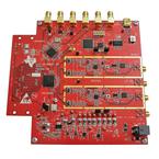
TSW308x Evaluation Module
Altera is a registered trademark of Altera Corporation.
Xilinx is a registered trademark of Xilinx Inc..
User's Guide
SLAU374B–December 2011–Revised May 2016
TSW308x Evaluation Module
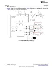
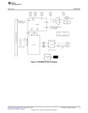
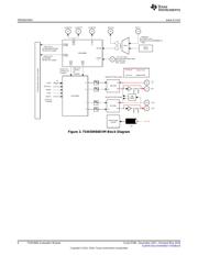
The Texas Instruments TSW308x evaluation module (EVM) provides a basic platform to evaluate the
DAC348x in a complete RF transmit signal chain. Along with the DAC348x, the EVM includes a
LMK04806B clock jitter cleaner and generator source, which provides the clocks required for the DAC and
the external pattern generator. The EVM also includes on-board TRF3705 I/Q modulators, which provide
IF-to-RF upconversion for basic transmitter evaluation. This EVM is ideally suited for mating with the
Texas Instruments TSW1400 pattern generation board for evaluating WCDMA, LTE, or other high-
performance modulation schemes.
Contents
1 Introduction ................................................................................................................... 3
1.1 Overview............................................................................................................. 3
1.2 EVM Block Diagram................................................................................................ 4
2 Software Control ............................................................................................................. 7
2.1 Installation Instructions............................................................................................. 7
2.2 Software Operation................................................................................................. 7
3 Basic Test Procedure with TSW1400 ................................................................................... 17
3.1 TSW1400 Overview............................................................................................... 17
3.2 Test Block Diagram for TSW1400 .............................................................................. 17
3.3 Test Setup Connection ........................................................................................... 18
3.4 TSW308x Example Setup Procedure........................................................................... 20
4 Basic Test Procedure with TSW3100 ................................................................................... 24
4.1 TSW3100 Overview............................................................................................... 24
4.2 Test Block Diagram for TSW3100 .............................................................................. 25
4.3 Test Setup Connection ........................................................................................... 26
4.4 TSW308x Example Setup Procedure........................................................................... 26
4.5 TSW3100 Example Setup Procedure .......................................................................... 27
5 Optional Configuration..................................................................................................... 28
5.1 Configuring the LMK04800 for Clock Distribution Mode ..................................................... 29
5.2 Configuring the LMK04800 for Single PLL (PLL2 Only) Mode.............................................. 29
5.3 Configuring the LMK04800 for Dual PLL (PLL1 + PLL2) Mode............................................. 29
6 Transmit Path Optional Configuration .................................................................................. 29
6.1 Shared LO Path (TSW3084 and TSW30H84 only)........................................................... 29
6.2 Additional RF amp and attenuator path ........................................................................ 29
List of Figures
1 TSW3084EVM Block Diagram............................................................................................. 4
2 TSW3085EVM Block Diagram............................................................................................. 5
3 TSW30H84EVM Block Diagram........................................................................................... 6
4 Input Tab Control Options – DAC348x.................................................................................... 8
5 PLL Configuration............................................................................................................ 9
6 Digital Tab Control Options – DAC348x................................................................................. 10
7 Output Tab Control Options – DAC348x................................................................................ 12
8 LMK04800 Tab Control Options.......................................................................................... 13
9 LMK04800 Advanced Settings Control Panel .......................................................................... 15