


下载
User's Guide
SLVU456A–May 2011– Revised June 2011
TPS22924EVM-532
This user's guide describes the characteristics, operation, and use of the TPS22924EVM-532 evaluation
module (EVM). This EVM demonstrates the Texas Instruments TPS22924 load switch with controlled turn
on. The input voltage range of the TPS22924 is 0.75 V to 3.6 V. An integrated charge pump biases the
NMOS switch to achieve a minimum switch ON resistance. The switch is controlled by an on/off input
(EN), which is capable of interfacing directly with low-voltage control signals. This user's guide includes
setup instructions, schematic diagram, bill of materials, and printed-circuit board layout drawings for the
EVM.
1 Introduction
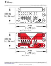
The TPS22924EVM-532 evaluation module (EVM) helps designers evaluate the operation and
performance of the TPS22924 load switch. The board features the small 6-pin CSP package for a small
solution size.
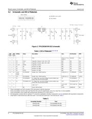
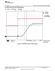
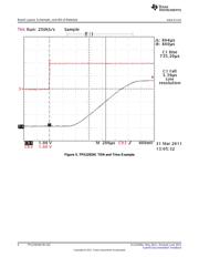
Table 1. TPS22924 VOUT Rise Time Options
EVM DEVICE Rise Time (µS) Typ. VIN(V)
HPA532-001 TPS22924B 100 3.6
HPA532-002 TPS22924C 840 3.6
1.1 Related Documentation From Texas Instruments
TPS22924, ULTRA-SMALL, LOW-INPUT-VOLTAGE, LOW r
ON
LOAD SWITCH data sheet (SLVSA52)
2 Setup
This section describes the jumpers and connectors on the EVM as well as how to properly connect, set
up, and use the TPS22924EVM-532.
2.1 J1/J3 – Input Connections
This is the connection for the leads from the input source. Connect the positive connection to the VIN J1
and the negative connection to the GND J3.
2.2 J4/J6 – Output Connections
This is the connection for the output of the TPS22924EVM. Connect the positive connection of the load to
the VOUT J4 and the negative connection to the GND J6.
2.3 JP3 – EN
This is the enable input for the device. Place a shorting jumper across the HI and EN pins of JP3 to
enable the integrated circuit (IC). Place a shorting jumper across the LO and EN pins of JP3 to disable the
IC. A shorting jumper must be installed on JP3 in either the ON or OFF positions, and EN must not be left
unconnected. An external enable source can be applied to the TPS22924 by removing the shunt and
connecting a signal to the center pin of JP3. EN ≥ 0.75V is required for the ACTIVE or ON state of the
device. A switching signal may also be used and connected at this point.
1
SLVU456A–May 2011–Revised June 2011 TPS22924EVM-532
Submit Documentation Feedback
Copyright © 2011, Texas Instruments Incorporated