
下载
TMS320C6454
www.ti.com
SPRS311I –APRIL 2006–REVISED MARCH 2012
TMS320C6454
Fixed-Point Digital Signal Processor
Check for Samples: TMS320C6454
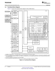
1 Features
12
– Interfaces to DDR2-533 SDRAM
• High-Performance Fixed-Point DSP (C6454)
– 32-Bit/16-Bit, 533-MHz (data rate) Bus
– 1.39-, 1.17-, and 1-ns Instruction Cycle Time
– 512M-Byte Total Addressable External
– 720-MHz, 850-MHz, and 1-GHz Clock Rate
Memory Space
– Eight 32-Bit Instructions/Cycle
• EDMA3 Controller (64 Independent Channels)
– 8000 MIPS/MMACS (16-Bits)
• 32-/16-Bit Host-Port Interface (HPI)
– Commercial Temperature [0°C to 90°C]
• 32-Bit 33-/66-MHz, 3.3-V Peripheral Component
– Extended Temperature [-40°C to 105°C]
Interconnect (PCI) Master/Slave Interface
• TMS320C64x+™ DSP Core
Conforms to PCI Local Bus Specification (v2.3)
– Dedicated SPLOOP Instruction
• One Inter-Integrated Circuit (I
2
C) Bus
– Compact Instructions (16-Bit)
• Two McBSPs
– Instruction Set Enhancements
• 10/100/1000 Mb/s Ethernet MAC (EMAC)
– Exception Handling
– IEEE 802.3 Compliant
• TMS320C64x+ Megamodule L1/L2 Memory
– Supports Multiple Media Independent
Architecture:
Interfaces (MII, GMII, RMII, and RGMII)
– 256K-Bit (32K-Byte) L1P Program Cache
– 8 Independent Transmit (TX) and
[Direct Mapped]
8 Independent Receive (RX) Channels
– 256K-Bit (32K-Byte) L1D Data Cache
• Two 64-Bit General-Purpose Timers,
[2-Way Set-Associative]
Configurable as Four 32-Bit Timers
– 8M-Bit (1048K-Byte) L2 Unified Mapped
• 16 General-Purpose I/O (GPIO) Pins
RAM/Cache [Flexible Allocation]
• System PLL and PLL Controller
– 256K-Bit (32K-Byte) L2 ROM
• Secondary PLL and PLL Controller, Dedicated
– Time Stamp Counter
to EMAC and DDR2 Memory Controller
• Endianess: Little Endian, Big Endian
• Advanced Event Triggering (AET) Compatible
• 64-Bit External Memory Interface (EMIFA)
• Trace-Enabled Device
– Glueless Interface to Asynchronous
• IEEE-1149.1 (JTAG™) Boundary-Scan-
Memories (SRAM, Flash, and EEPROM) and
Compatible
Synchronous Memories (SBSRAM, ZBT
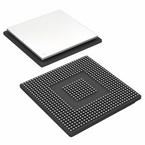
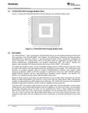
• 697-Pin Ball Grid Array (BGA) Package
SRAM)
(CTZ, GTZ, or ZTZ Suffix), 0.8-mm Ball Pitch
– Supports Interface to Standard Sync Devices
• 0.09-μm/7-Level Cu Metal Process (CMOS)
and Custom Logic
• 3.3-/1.8-/1.5-V I/Os,
(FPGA, CPLD, ASICs, etc.)
1.25-/1.2-V Internal
– 32M-Byte Total Addressable External
• Pin-Compatible with the TMS320C6455 Fixed-
Memory Space
Point Digital Signal Processor
• DDR2 Memory Controller
1
Please be aware that an important notice concerning availability, standard warranty, and use in critical applications of
Texas Instruments semiconductor products and disclaimers thereto appears at the end of this data sheet.
2All trademarks are the property of their respective owners.
PRODUCTION DATA information is current as of publication date. Products conform to
Copyright © 2006–2012, Texas Instruments Incorporated
specifications per the terms of the Texas Instruments standard warranty. Production
processing does not necessarily include testing of all parameters.
页面指南