

下载
TMS320C6452
www.ti.com
SPRS371F –OCTOBER 2007–REVISED APRIL 2012
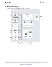
TMS320C6452 Digital Signal Processor
Check for Samples: TMS320C6452
1 Features
1
– 256K-bit (32K-byte) L1P Program RAM/Cache
• High-Performance Digital Media Processor
[Direct Mapped]
– 720-MHz, 900-MHz C64x+™ Clock Rates
– 256K-bit (32K-byte) L1D Data RAM/Cache
– 1.39 ns (-720), 1.11 ns (-900) Instruction
[2-Way Set-Associative]
Cycle Time
– 1408KB L2 Unified Mapped RAM/Cache
– 5760, 7200 MIPS
[Flexible Allocation]
– Eight 32-Bit C64x+ Instructions/Cycle
• Supports Little Endian Mode Only
– Fully Software-Compatible With C64x/Debug
• External Memory Interfaces (EMIFs)
– Commercial Temperature Ranges (-720, -900
– 32-Bit DDR2 SDRAM Memory Controller With
only)
512M-Byte Address Space (1.8-V I/O)
– Industrial Temperature Ranges (-720, -900
– Asynchronous 16-Bit Wide EMIF (EMIFA)
only)
• Up to 128M-Byte Total Address Reach
• VelociTI.2™ Extensions to VelociTI™
• 64M-Byte Address Reach per CE Space
Advanced Very-Long-Instruction-Word (VLIW)
TMS320C64x+™ DSP Core – Glueless Interface to Asynchronous
Memories (SRAM, Flash, and EEPROM)
– Eight Highly Independent Functional Units
With VelociTI.2 Extensions: – Synchronous Memories (SBSRAM and ZBT
SRAM)
• Six ALUs (32-/40-Bit), Each Supports
Single 32-bit, Dual 16-bit, or Quad 8-bit – Supports Interface to Standard Sync Devices
Arithmetic per Clock Cycle and Custom Logic (FPGA, CPLD, ASICs,
etc.)
• Two Multipliers Support Four 16 x 16-bit
Multiplies (32-bit Results) per Clock Cycle • Enhanced Direct-Memory-Access (EDMA)
or Eight 8 x 8-bit Multiplies (16-Bit Controller (64 Independent Channels)
Results) per Clock Cycle
• 3-Port Gigabit Ethernet Switch Subsystem
– Load-Store Architecture With Non-Aligned
• Four 64-Bit General-Purpose Timers (Each
Support
Configurable as Two 32-Bit Timers)
– 64 32-bit General-Purpose Registers
• One UART (With RTS and CTS Flow Control)
– Instruction Packing Reduces Code Size
• One 4-wire Serial Port Interface (SPI) With Two
– All Instructions Conditional Chip-Selects
– Additional C64x+™ Enhancements • Master/Slave Inter-Integrated Circuit (I2C
Bus™)
• Protected Mode Operation
• Two Telecom Serial Interface Ports (TSIP0/1)
• Exceptions Support for Error Detection
and Program Redirection • Multichannel Audio Serial Port (McASP)
• Hardware Support for Modulo Loop Auto- – Ten Serializers and SPDIF (DIT) Mode
Focus Module Operation
• 16/32-Bit Host-Port Interface (HPI)
• C64x+ Instruction Set Features
• Advanced Event Triggering (AET) Compatible
– Byte-Addressable (8-/16-/32-/64-bit Data)
• 32-Bit 33-/66-MHz, 3.3-V Peripheral Component
– 8-bit Overflow Protection Interconnect (PCI) Master/Slave Interface
Conforms to PCI Specification 2.3
– Bit-Field Extract, Set, Clear
• VLYNQ™ Interface (FPGA Interface)
– Normalization, Saturation, Bit-Counting
• On-Chip ROM Bootloader
– VelociTI.2 Increased Orthogonality
• Individual Power-Saving Modes
– C64x+ Extensions
• Flexible PLL Clock Generators
• Compact 16-bit Instructions
• IEEE-1149.1 (JTAG™) Boundary-Scan-
• Additional Instructions to Support
Compatible
Complex Multiplies
• 32 General-Purpose I/O (GPIO) Pins
• C64x+ L1/L2 Memory Architecture
(Multiplexed With Other Device Functions)
1
Please be aware that an important notice concerning availability, standard warranty, and use in critical applications of
Texas Instruments semiconductor products and disclaimers thereto appears at the end of this data sheet.
PRODUCTION DATA information is current as of publication date. Products conform to
Copyright © 2007–2012, Texas Instruments Incorporated
specifications per the terms of the Texas Instruments standard warranty. Production
processing does not necessarily include testing of all parameters.
页面指南