
下载

SPRS294B − OCTOBER 2005 − REVISED JUNE 2006
1
POST OFFICE BOX 1443 • HOUSTON, TEXAS 77251−1443
D Highest-Performance Floating-Point Digital
Signal Processor (DSP): TMS320C6713B
− Eight 32-Bit Instructions/Cycle
− 32/64-Bit Data Word
− 300-, 225-, 200-MHz (GDP and ZDP), and
225-, 200-, 167-MHz (PYP) Clock Rates
− 3.3-, 4.4-, 5-, 6-Instruction Cycle Times
− 2400/1800, 1800/1350, 1600/1200, and
1336/1000 MIPS/MFLOPS
− Rich Peripheral Set, Optimized for Audio
− Highly Optimized C/C++ Compiler
− Extended Temperature Devices Available
D Advanced Very Long Instruction Word
(VLIW) TMS320C67x DSP Core
− Eight Independent Functional Units:
− 2 ALUs (Fixed-Point)
− 4 ALUs (Floating-/Fixed-Point)
− 2 Multipliers (Floating-/Fixed-Point)
− Load-Store Architecture With 32 32-Bit
General-Purpose Registers
− Instruction Packing Reduces Code Size
− All Instructions Conditional
D Instruction Set Features
− Native Instructions for IEEE 754
− Single- and Double-Precision
− Byte-Addressable (8-, 16-, 32-Bit Data)
− 8-Bit Overflow Protection
− Saturation; Bit-Field Extract, Set, Clear;
Bit-Counting; Normalization
D L1/L2 Memory Architecture
− 4K-Byte L1P Program Cache
(Direct-Mapped)
− 4K-Byte L1D Data Cache (2-Way)
− 256K-Byte L2 Memory Total: 64K-Byte
L2 Unified Cache/Mapped RAM, and
192K-Byte Additional L2 Mapped RAM
D Device Configuration
− Boot Mode: HPI, 8-, 16-, 32-Bit ROM Boot
− Endianness: Little Endian, Big Endian
D 32-Bit External Memory Interface (EMIF)
− Glueless Interface to SRAM, EPROM,
Flash, SBSRAM, and SDRAM
− 512M-Byte Total Addressable External
Memory Space
D Enhanced Direct-Memory-Access (EDMA)
Controller (16 Independent Channels)
D 16-Bit Host-Port Interface (HPI)
D Two McASPs
− Two Independent Clock Zones Each
(1 TX and 1 RX)
− Eight Serial Data Pins Per Port:
Individually Assignable to any of the
Clock Zones
− Each Clock Zone Includes:
− Programmable Clock Generator
− Programmable Frame Sync Generator
− TDM Streams From 2-32 Time Slots
− Support for Slot Size:
8, 12, 16, 20, 24, 28, 32 Bits
− Data Formatter for Bit Manipulation
− Wide Variety of I2S and Similar Bit
Stream Formats
− Integrated Digital Audio Interface
Transmitter (DIT) Supports:
− S/PDIF, IEC60958-1, AES-3, CP-430
Formats
− Up to 16 transmit pins
− Enhanced Channel Status/User Data
− Extensive Error Checking and Recovery
D Two Inter-Integrated Circuit Bus (I
2
C Bus)
Multi-Master and Slave Interfaces
D Two Multichannel Buffered Serial Ports:
− Serial-Peripheral-Interface (SPI)
− High-Speed TDM Interface
− AC97 Interface
D Two 32-Bit General-Purpose Timers
D Dedicated GPIO Module With 16 pins
(External Interrupt Capable)
D Flexible Phase-Locked-Loop (PLL) Based
Clock Generator Module
D IEEE-1149.1 (JTAG
†
)
Boundary-Scan-Compatible
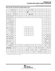
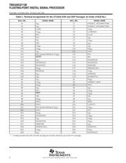
D 208-Pin PowerPAD PQFP (PYP)
D 272-BGA Packages (GDP and ZDP)
D 0.13-µm/6-Level Copper Metal Process
− CMOS Technology
D 3.3-V I/Os, 1.2
‡
-V Internal (GDP/ZDP/ PYP)
D 3.3-V I/Os, 1.4-V Internal (GDP/ZDP) [300
MHz]
Please be aware that an important notice concerning availability, standard warranty, and use in critical applications o
f
Texas Instruments semiconductor products and disclaimers thereto appears at the end of this data sheet.
Copyright 2006, Texas Instruments Incorporated
TMS320C67x and PowerPAD are trademarks of Texas Instruments.
I
2
C Bus is a trademark of Philips Electronics N.V. Corporation
All trademarks are the property of their respective owners.
†
IEEE Standard 1149.1-1990 Standard-Test-Access Port and Boundary Scan Architecture.
‡
These values are compatible with existing 1.26-V designs.
! " #$%! " &$'(#! )!%*
)$#!" # ! "&%##!" &% !+% !%" %," "!$%!"
"!)) -!.* )$#! &#%""/ )%" ! %#%""(. #($)%
!%"!/ (( &%!%"*