

下载
TLV2556
SLAS355A – DECEMBER 2001 – REVISED SEPTEMBER 2002
12-BIT, 200-KSPS, 11 CHANNEL, LOW POWER, SERIAL ADC
WITH INTERNAL REFERENCE
1
www.ti.com
FEATURES
D
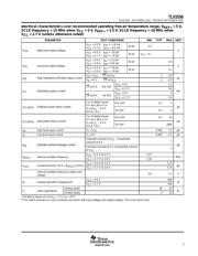
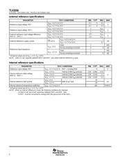
12-Bit-Resolution A/D Converter
D Up to 200-KSPS (150-KSPS for 3 V)
Throughput Bit With 12-Output Mode Over
Operating Temperature Range
D 11 Analog Input Channels
D 3 Built-In Self-Test Modes
D Programmable Reference (2.048/4.096 V
Internal, External)
D Inherent Sample and Hold Function
D Linearity Error ...±1 LSB Max
D On-Chip Conversion Clock
D Programmable Conversion Status Output: INT
or EOC
D Unipolar or Bipolar Output Operation
D Programmable MSB or LSB First
D Programmable Power Down
D Programmable Output Data Length
D SPI Compatible Serial Interface With I/O Clock
Frequencies up to 15 MHz (CPOL=0, CPHA=0)
APPLICATIONS
D
Industrial Process Control
D Portable Data Logging
D Battery Powered Instruments
D Automotive
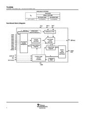
DESCRIPTION
The TLV2556 is a 12-bit, switched-capacitor,
successive-approximation, analog-to-digital converter.
The ADC has three control inputs [chip select (CS
), the
input-output clock, and the address/control input
(DATAIN)], designed for communication with the serial
port of a host processor or peripheral through a serial
3-state output.
In addition to the high-speed converter and versatile
control capability, the device has an on-chip 14-channel
multiplexer that can select any one of 11 inputs or any
one of three internal self-test voltages using
configuration register 1. The sample-and-hold function
is automatic. At the end of conversion, when
programmed as EOC, the pin 19 output goes high to
indicate that conversion is complete. If pin 19 is
programmed as INT
, the signal goes low when the
conversion is complete. The converter incorporated in
the device features differential, high-impedance
reference inputs that facilitate ratiometric conversion,
scaling, and isolation of analog circuitry from logic and
supply noise. A switched-capacitor design allows low-
error conversion over the full operating temperature
range. An internal reference is available and its voltage
level is programmable via configuration register 2
(CFGR2).
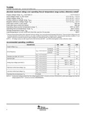
The TLV2556I is characterized for operation from
T
A
= –40°C to 85°C. See available options table for
package options.
PRODUCTION DATA information is current as of publication date.
Products conform to specifications per the terms of Texas Instruments
standard warranty. Production processing does not necessarily include
testing of all parameters.
Copyright 2002, Texas Instruments Incorporated
Please be aware that an important notice concerning availability, standard warranty, and use in critical applications of
Texas Instruments semiconductor products and disclaimers thereto appears at the end of this data sheet.
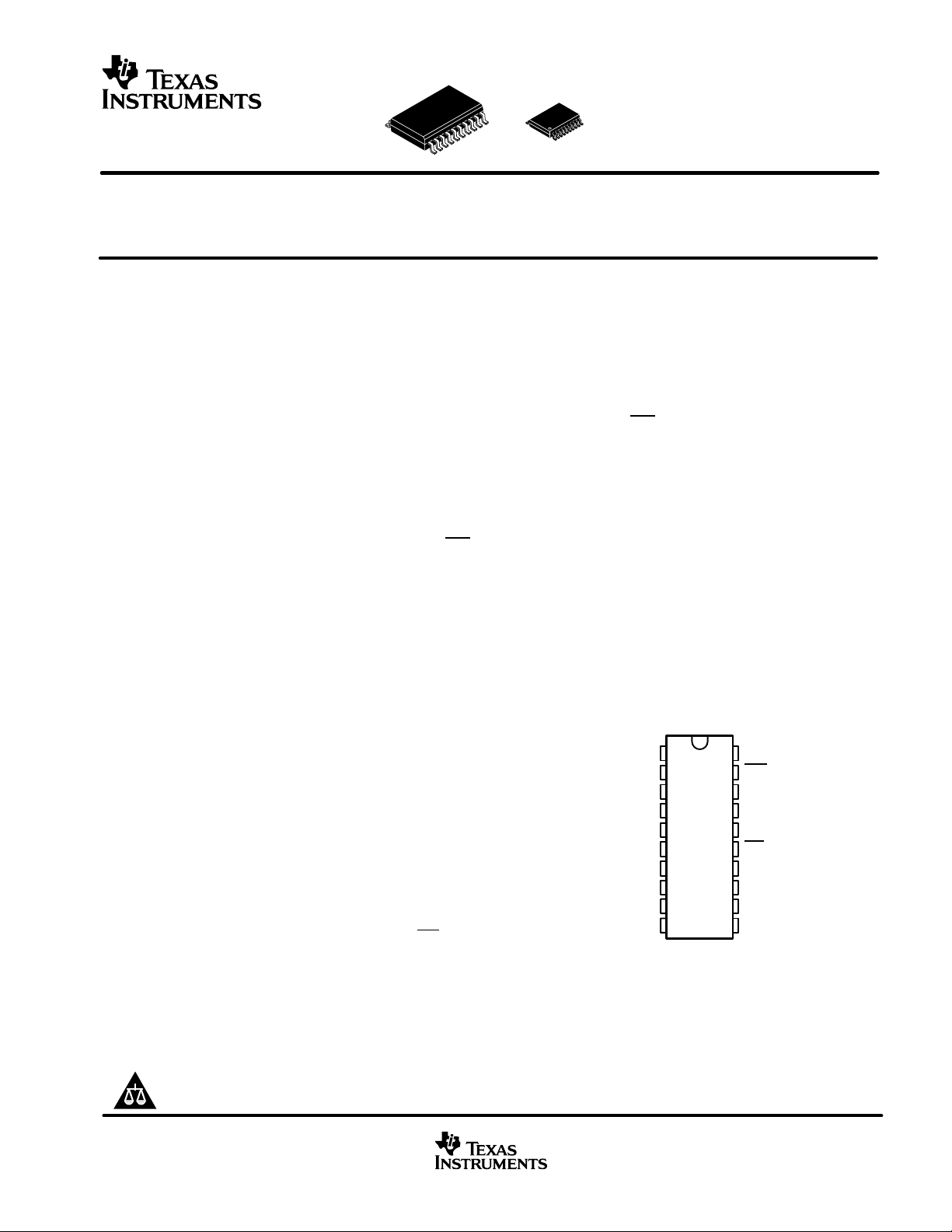
1
2
3
4
5
6
7
8
9
10
20
19
18
17
16
15
14
13
12
11
AIN0
AIN1
AIN2
AIN3
AIN4
AIN5
AIN6
AIN7
AIN8
GND
V
CC
INT/EOC
I/O CLOCK
DATA IN
DATA OUT
CS
REF+
REF–
AIN10
AIN9
(TOP VIEW)
PW AND DW PACKAGE