


Application Report
SLVA531A–February 2013–Revised September 2013
TLK1XX Design and Layout Guide
AviadYarmakov....................................................................................................... IndustrialInterface
ABSTRACT
Many times when approaching a new design, significant time and effort can be saved by applying correct
and recommended design guidelines already in the planning phase. The purpose of this document is to
supply these guidelines to the engineer working with the TLK family of products; saving time, effort, and
cost, and decreasing time to market for their solution.
Contents
1 Introduction .................................................................................................................. 3
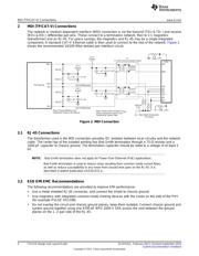
2 MDI (TP/CAT-V) Connections ............................................................................................. 4
2.1 RJ-45 Connections ................................................................................................ 4
2.2 ESD EMI EMC Recommendations .............................................................................. 4
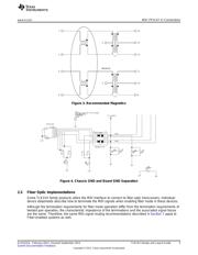
2.3 Fiber Optic Implementations ...................................................................................... 5
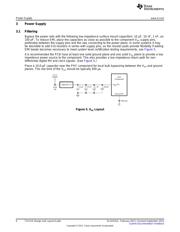
3 Power Supply ................................................................................................................ 6
3.1 Filtering .............................................................................................................. 6
3.2 Single-Supply Operation .......................................................................................... 7
3.3 Dual-Supply Operation ............................................................................................ 8
3.4 I/O Voltage Supply ................................................................................................. 8
3.5 CT Supply ........................................................................................................... 8
4 MAC Interfaces .............................................................................................................. 9
4.1 Media Independent Interface (MII) ............................................................................... 9
4.2 Reduced Media Independent Interface (RMII) ................................................................ 10
4.3 Termination Requirement ....................................................................................... 10
4.4 Recommended Maximum Trace Length ...................................................................... 11
5 Clock Requirements ....................................................................................................... 11
5.1 External Oscillator Clock Source ............................................................................... 11
5.2 Crystal Clock Source ............................................................................................. 12
5.3 Oscillator or Crystal .............................................................................................. 12
6 LED and Non-LED Strap Pins ........................................................................................... 13
7 PCB Layout Considerations .............................................................................................. 14
7.1 Calculating Impedance .......................................................................................... 15
7.2 PCB Layer Stacking .............................................................................................. 16
8 Magnetics ................................................................................................................... 18
9 ESD Design Guidelines ................................................................................................... 19
9.1 Board Design Guidelines ........................................................................................ 19
9.2 Board Layout Guidelines ........................................................................................ 20
10 Reset Operation ........................................................................................................... 22
10.1 Hardware Reset .................................................................................................. 22
10.2 POR_BYPASS mode (TLK110 only) .......................................................................... 22
10.3 Software Reset ................................................................................................... 22
11 Schematics Example ...................................................................................................... 23
12 Other Applicable Documents ............................................................................................. 29
List of Figures
1 Typical Application.......................................................................................................... 3
1
SLVA531A–February 2013–Revised September 2013 TLK1XX Design and Layout Guide
Submit Documentation Feedback
Copyright © 2013, Texas Instruments Incorporated