

下载
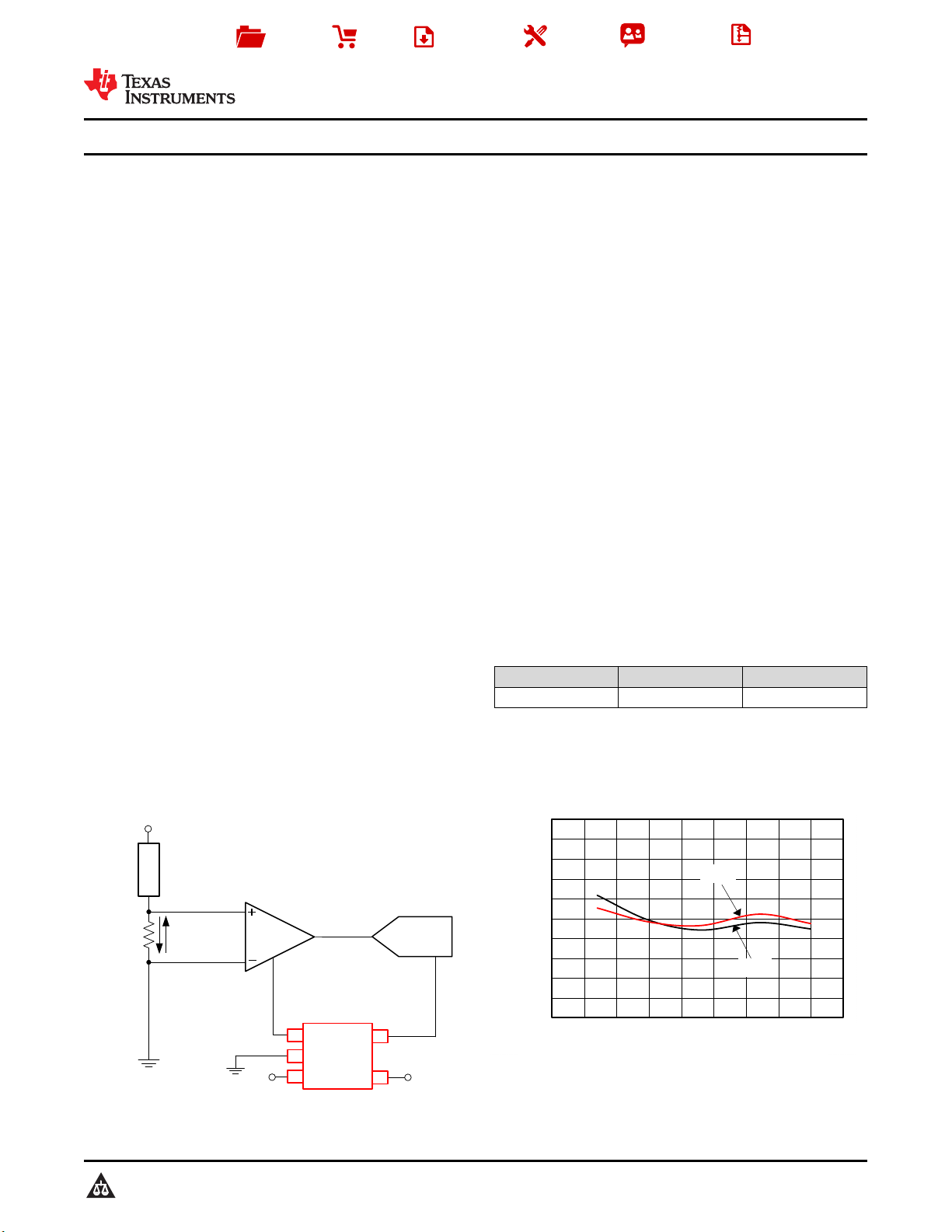
INA213
V
IN
REF2030
V
REF
3.0 V
V
BIAS
1.5 V
EN
ADC
GND
LOAD
I
SENSE
R
SHUNT
V
IN-
V
IN+
REF
V
OUT
Power
Supply
-0.05
-0.04
-0.03
-0.02
-0.01
0
0.01
0.02
0.03
0.04
0.05
±75 ±50 ±25 0 25 50 75 100 125 150
Output Voltage Accuracy (%)
Temperature (ƒC)
C001
V
REF
V
BIAS
Product
Folder
Order
Now
Technical
Documents
Tools &
Software
Support &
Community
Reference
Design
An IMPORTANT NOTICE at the end of this data sheet addresses availability, warranty, changes, use in safety-critical applications,
intellectual property matters and other important disclaimers. PRODUCTION DATA.
REF2025
,
REF2030
,
REF2033
,
REF2041
SBOS600C –MAY 2014–REVISED JANUARY 2017
REF20xx Low-Drift, Low-Power, Dual-Output, V
REF
and V
REF
/ 2 Voltage References
1
1 Features
1
• Two Outputs, V
REF
and V
REF
/ 2, for Convenient
Use in Single-Supply Systems
• Excellent Temperature Drift Performance:
– 8 ppm/°C (max) from –40°C to 125°C
• High Initial Accuracy: ±0.05% (max)
• V
REF
and V
BIAS
Tracking over Temperature:
– 6 ppm/°C (max) from –40°C to 85°C
– 7 ppm/°C (max) from –40°C to 125°C
• Microsize Package: SOT23-5
• Low Dropout Voltage: 10 mV
• High Output Current: ±20 mA
• Low Quiescent Current: 360 μA
• Line Regulation: 3 ppm/V
• Load Regulation: 8 ppm/mA
2 Applications
• Digital Signal Processing:
– Power Inverters
– Motor Controls
• Current Sensing
• Industrial Process Controls
• Medical Equipment
• Data Acquisition Systems
• Single-Supply Systems
3 Description
Applications with only a positive supply voltage often
require additional stable voltage in the middle of the
analog-to-digital converter (ADC) input range to bias
input bipolar signals. The REF20xx provides a
reference voltage (V
REF
) for the ADC and a second
highly-accurate voltage (V
BIAS
) that can be used to
bias the input bipolar signals.
The REF20xx offers excellent temperature drift
(8 ppm/°C, max) and initial accuracy (0.05%) on both
the V
REF
and V
BIAS
outputs while operating at a
quiescent current less than 430 µA. In addition, the
V
REF
and V
BIAS
outputs track each other with a
precision of 6 ppm/°C (max) across the temperature
range of –40°C to 85°C. All these features increase
the precision of the signal chain and decrease board
space, while reducing the cost of the system as
compared to a discrete solution. Extremely low
dropout voltage of only 10 mV allows operation from
very low input voltages, which can be very useful in
battery-operated systems.
Both the V
REF
and V
BIAS
voltages have the same
excellent specifications and can sink and source
current equally well. Very good long-term stability and
low noise levels make these devices ideally-suited for
high-precision industrial applications.
Device Information
(1)
PART NAME PACKAGE BODY SIZE (NOM)
REF20xx SOT (5) 2.90 mm × 1.60 mm
(1) For all available packages, see the orderable addendum at
the end of the datasheet.
space
space
Application Example V
REF
and V
BIAS
vs Temperature
页面指南