

下载

© Semiconductor Components Industries, LLC, 2012
November, 2012 − Rev. 4
1 Publication Order Number:
EVBUM2049/D
NCP1611GEVB
160-W, Wide Mains, PFC
Stage Driven by the
NCP1611 Evaluation Board
User's Manual
Introduction
Housed in a SO-8 package, The NCP1611 is designed to
drive PFC boost stages in so-called Current Controlled
Frequency Fold-back (CCFF). In this mode, the circuit
classically operates in Critical conduction Mode (CrM)
when the inductor current exceeds a programmable value.
When the current is below this preset level, the NCP1611
linearly decays the frequency down to about 20 kHz when
the current is nearly zero. CCFF maximizes the efficiency
throughout the load range. Incorporating protection features
for rugged operation, it is furthermore ideal in systems
where cost-effectiveness, reliability, low stand-by power
and high-efficiency are the key requirements.
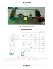
Extremely slim, the NCP1611 evaluation board is
designed to be less than 13 mm high. This low-profile PFC
stage is intended to deliver 160 W under a 390 V output
voltage from a wide mains input. This is a PFC boost
converter as used in Flat TVs, High Power LED Street Light
power supplies, and all-in-one computer supplies. The
evaluation board embeds the NCP1611 B-version which is
best appropriate for the self-biased configuration. The board
is also configurable to have the NCP1611 powered from an
external power source. In this case, apply a V
CC
voltage that
exceeds the NCP1611B start-up level (18.2 V max) to ensure
the circuit start of operation or solder the NCP1611A
instead. The A-version start-up level is lower than 11.25 V
to allow the circuit powering from a 12 V rail. Both versions
feature a large V
CC
operating range (from 9.5 V up to 35 V).
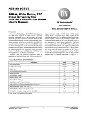
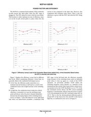
Table 1. ELECTRICAL SPECIFICATIONS
Description Value Units
Input Voltage Range 90-265 Vrms
Line Frequency Range 45 to 66 Hz
Output Power 160 W
Minimum Output Load Current(s) 0 Adc
Number of Outputs 1
Nominal Output Voltage 390 Vdc
Maximum Startup Time < 3 s
No-Load Power (115 V
rms
) < 250 mW
Target Efficiency at Full Load (115 V
rms
) 95 %
Load Conditions For Efficiency Measurements (10%, 20%,..) 10-100 %
Minimum Efficiency At 20% Load, 115 V
rms
93 %
Minimum PF Over The Line Range At Full Load 95 %
Hold-Up Time (the output voltage remaining above 300 V) > 10 ms
Peak To Peak Low Frequency Output Ripple < 8 %
http://onsemi.com
EVAL BOARD USER’S MANUAL