
下载

© Semiconductor Components Industries, LLC, 2012
September, 2012 − Rev. 0
1 Publication Order Number:
EVBUM2138/D
NCP4354AADAPGEVB
65 W Off-Line Adapter
Featuring Very Low
No-Load Power
Consumption Evaluation
Board User's Manual
Overview
When designing an offline Ac-Dc power adapter, one key
consideration is the power consumption in standby mode.
Standby power consumption, also sometimes referred to as
vampire power or phantom load, is the power consumed by
electronic devices when they are switched off, but still
plugged into the wall. It is estimated that standby power
accounts for nearly 10% of the energy usage in the average
American home. One common contributor to vampire
power in the home is notebook adapters. These adapters
spend a lot of time left underneath desks with the notebook
computer disconnected or powered off. The following
design note features the latest techniques for minimizing the
standby power consumption of a 65 W notebook adapter.
When focusing on the no load power consumption of an
adapter design, the key losses need to be identified.
Switching losses and circuit biasing must be minimized or
eliminated completely. The latest technique for minimizing
losses during no load is to turn off the Ac-Dc controller and
allow the output voltage to drop. Because the adapter is not
supplying power, a drop in output voltage is viewed as
acceptable. The following design utilizes the NCP1246
flyback controller and the NCP4354A secondary side
controller to realize this technique. Both controllers have
built-in features focused on minimizing no load input power
consumption. Primary side flyback controller NCP1246 is
a fixed frequency current mode controller featuring
dynamic self supply. It also supports OFF mode and
integrated active X2 capacitor discharge feature, which
significantly reduces input power at very light load and no
load conditions. NCP1246 includes frequency fold-back
and skip mode to provide high efficiency in light load.
Secondary side controller NCP4354A provides output
voltage and current regulation (CCCV operation of whole
SMPS), very light load condition detection, OFF mode
control and indication LED driver. The NCP4354A is
specially design for use in tandem with the NCP1246,
detecting no load conditions and triggering OFF mode via
the NCP1246 FB pin.
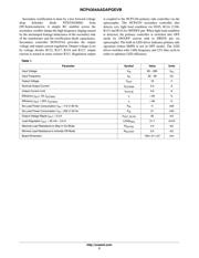
Key Features
• Constant Voltage Constant Current Regulation (CCCV)
• Very Low Input Power at Light and No Load
• High Efficiency Across the Entire Load Range
• Overpower Protection
• Universal Mains Operation
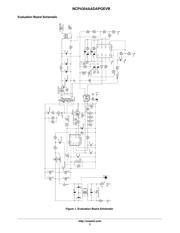
Circuit Description
The primary side uses a flyback topology, providing the
advantage of a cost effective power stage design. The power
stage operates in both CCM (continuous conduction mode)
and DCM (discontinuous conduction mode), allowing it to
accept a wide universal input voltage range. The CCM
operation provides desired full load performance with good
efficiency and low ripple of primary current. The DCM
operation then permits an increase of efficiency under the
light load conditions, by decreasing the switching losses.
The device switches at 65 kHz which represents a good
trade-off between switching losses and magnetic core size.
The adapter primary side consists of several important
sections. The first is an input EMI filter to reduce the
conducted EMI to the ac line at the input of the adapter. The
EMI filter is formed by common-mode inductors L3 and
capacitors C1, C2, C3 and C11 with differential mode
inductor L2. The varistor R7 is used to protect the adapter
against the line overvoltage peaks. When the power supply
is disconnected from the AC mains, X capacitors C2, C13
and Y capacitors C3 and C4 are discharged through HV pin
via the following path: rectifying diodes D101, D103, surge
protection T network R100, R101 and C100. This feature
replaces commonly used discharging resistors and saves
approximately 25 mW of input power consumption at
230 Vac. The next block is the rectifier with bulk capacitor.
The main power stage of the flyback converter utilizes the
low R
DSon
MOSFET SPP11N60C3 along with a custom
designed transformer TR1 KA5038-BL from Coilcraft. The
detailed design procedure of a flyback adapter can be found
in the application note AND8461/D at ON Semiconductor
website: http://www.onsemi.com
.
http://onsemi.com
EVAL BOARD USER’S MANUAL