

下载
© Semiconductor Components Industries, LLC, 2015
May, 2015 − Rev. 2
1 Publication Order Number:
NB3N51054/D
NB3N51054
3.3 V, Crystal to 100 MHz
Quad HCSL/LVDS PCIe
Clock Generator
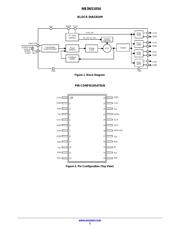
The NB3N51054 is a precision, low phase noise clock generator that
supports PCI Express requirements. The device accepts a 25 MHz
fundamental mode parallel resonant crystal or a 25 MHz reference
clock signal and generates four differential HCSL/LVDS outputs (See
Figure 7 for LVDS interface) at 100 MHz clock frequency with
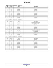
maximum skew of 40 ps. Through I
2
C interface, NB3N51054
provides selectable spread spectrum options of −0.35% and −0.5% for
applications demanding low Electromagnetic Interface (EMI) as well
as optimum performance with no spread option. The I
2
C interface
further enables control of each output and they can be enabled/
disabled individually.
Features
• Uses 25 MHz Fundamental Crystal or Reference Clock Input
• Four Low Skew HCSL or LVDS Outputs
• I
2
C Support with Read Back Capability
• Spread of −0.35%, −0.5% and No Spread
• Individual Output Enable/Disable Control through I
2
C
• PCIe Gen 1, Gen 2, Gen 3 Compliant
• Typical Phase Jitter @ 100 MHz (Integrated 12 kHz to 20 MHz):
0.5 ps
• Typical Cycle−Cycle Jitter @ 100 MHz (10k cycles): 20 ps
• Phase Noise @ 100 MHz:
Offset Noise Power
100 Hz −104 dBc/Hz
1 kHz −121 dBc/Hz
10 kHz −131 dBc/Hz
100 kHz −136 dBc/Hz
1 MHz −140 dBc/Hz
10 MHz −155 dBc/Hz
• Operating Power Supply: 3.3 V ± 5%
• Industrial Temperature Range: −40°C to 85°C
• Functionally Compatible with ICS841S104I with enhanced
performance
• These are Pb−Free Devices
Application
• Networking
• Consumer
• Computing and Peripherals
• Industrial Equipment
• PCIe Clock Generation Gen 1, Gen 2 and Gen 3
End Products
• Switch and Router
• Set Top Box, LCD TV
• Servers, Desktop Computers
• Automated Test Equipment
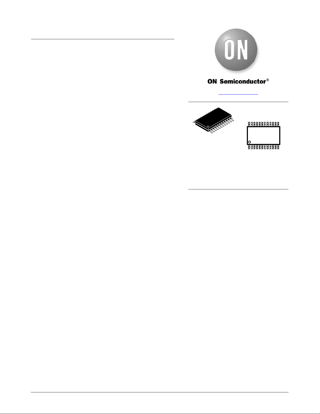
MARKING
DIAGRAM
TSSOP−24
CASE 948H
www.onsemi.com
See detailed ordering and shipping information in the package
dimensions section on page 14 of this data sheet.
ORDERING INFORMATION
NB3N5
1054G
ALYW
A = Assembly Location
L = Wafer Lot
Y = Year
W = Work Week
G = Pb−Free Package
页面指南