
下载
Semiconductor Components Industries, LLC, 2012
August, 2012 − Rev. 1
1 Publication Order Number:
EVBUM2133/D
NCP1216AFORWGEVB
Implementing a DC/DC
Single‐ended Forward
Converter with the
NCP1216A Evaluation
Board User's Manual
Introduction
This document describes how the NCP1216A controller
can be used to design a DC/DC single-ended forward
converter suitable for telecommunication applications. The
requirements for the converter are as follows:
Input Voltage Range from 36 V to 72 VDC
Continuous Output Power Greater than 30 W for a 12 V
Output Voltage
Small PCB Dimensions
Efficiency Greater then 85%
Input to Output Isolation Voltage of 1500 V
The NCP1216A controller is an attractive solution for this
application, due to the following features:
50% Maximum Duty Cycle Operation
Forward converters usually limit the maximum duty
cycle to 50%. Since the voltage reset is constrained to
be equal to the input voltage (1:1 reset ratio), it is not
desirable to exceed 50% DC to avoid saturating the
transformer core.
No Auxiliary Winding Operation
The DSS (Dynamic Self-supply) function allows
the NCP1216A derive power directly from the HV
line without having to supply V
CC
either from the
secondary output inductance (creepage distance and
isolation issues) or via an auxiliary winding delivering
a variable voltage of N V
in
.
500 mA Peak Current Capability
The NCP1216A can drive a MOSFET directly without
any additional driver stage. If the selected MOSFET
gate charge would overload the DSS capability, then an
auxiliary winding could be used solely to supply the
driver pulses.
Current-mode Operation
Cycle-by-cycle primary current monitoring eliminates
any overcurrent situations, e.g. resulting from a
secondary short-circuit.
Direct Optocoupler Connection
In applications where the input to output isolation is
required, a direct connection eases the design stage,
saving external components.
Extremely Low No-load Power Consumption
Extremely low consumption in no-load operation is a
great advantage of the NCP1216A controller. Today’s
maximum stand-by consumption standards can be
easily met if this function is used.
Short-circuit Protection
By monitoring the activity on the feedback line,
the NCP1216A simplifies the task of secondary side
short-circuit protection. Coupling problems are
eliminated thanks to this feature and the DSS
implementation.
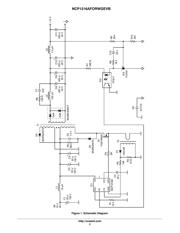
The 35 W DC/DC Converter Board Specifications
The schematic of the proposed converter is shown in
Figure 1. This converter has the following specifications:
Minimum Input Voltage 36 VDC
Maximum Input Voltage 72 VDC
Output Voltage 12 VDC
Continued Output Current 3.0 A
Operating Frequency 100 kHz
No-load Consumption at 48 V 1.8 mA
Maximum Ambient Temperature 70C
http://onsemi.com
EVAL BOARD USER’S MANUAL