
下载
© Semiconductor Components Industries, LLC, 2014
July, 2014 − Rev. 1
1 Publication Order Number:
EVBUM2241/D
NB7L1008MNGEVB
NB7L1008MNG Evaluation
Board User's Manual
Introduction
The NB7L1008 is a high performance differential
1:8 Clock/Data fanout buffer that operates up to
12 Gbps/7 GHz with a 2.5 V or 3.3 V power supply.
ON Semiconductor has developed a “universal” QFN−32
evaluation board and configured it for the NB7L1008. This
evaluation board was designed to provide a flexible and
convenient platform to quickly evaluate, characterize and
verify the operation of the NB7L1008.
This evaluation board manual contains:
• Information on the NB7L1008 Evaluation Board
• Test and Measurement Setup Procedures
This manual should be used in conjunction with the device
datasheet, which contains full technical details on the device
specifications and operation.
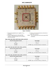
Board Layout
The NB7L1008 Evaluation Board provides a high
bandwidth, 50-W controlled impedance environment and is
implemented in one layer.
Layer Stack
L1 (Rogers)
High-performance SMA connectors are provided for all
high-speed input & output signal access.
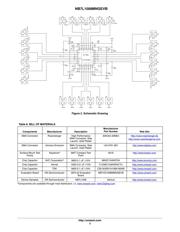
Evaluation Board Assembly Instructions
The QFN−32 evaluation board is designed for
characterizing devices in a 50-W laboratory environment
using high bandwidth equipment.
Output Loading/Termination
LVPECL Outputs
Table 1. DIFFERENTIAL INPUTS DRIVEN SINGLE – ENDED (Notes 1 & 2)
Symbol Characteristic Min Typ Max Unit
V
IH
Single – Ended Input High Voltage V
th
+ 75 − V
CC
mV
V
IL
Single – Ended Input Low Voltage V
EE
− V
th
− 100 mV
V
th
Input Threshold Reference Voltage Range V
EE
+ 1100 − V
CC
− 100 mV
V
ISE
Single – Ended Input Voltage (V
IH
– V
IL
) 200 − 1200 mV
1. V
th
, V
IH
, V
IL
and V
ISE
parameters must be complied with simultaneously.
2. V
th
is applied to the complementary input when operating in single-ended mode.
Table 2. DIFFERENTIAL INPUTS DRIVEN DIFFERENTIALLY (IN, INB) (Note 3)
Symbol
Characteristic Min Typ Max Unit
V
IHD
Differential Input High Voltage V
EE
+ 1100 − V
CC
mV
V
ILD
Differential Input Low Voltage V
EE
− V
IHD
− 100 mV
V
ID
Differential Input Voltage (V
IHD
– V
ILD
) 100 − 1200 mV
I
IH
Input High Current −150 40 +150
mA
I
IL
Input Low Current −150 5 +150
mA
3. V
IHD
, V
ILD
, V
ID
and V
CMR
parameters must be complied with simultaneously.
If the input signals to the NB7L1008 require termination,
internal 50-W resistors are provided via the VT pin and
grounded using a SMA grounding plug then and should be
stimulated with the appropriate voltage levels.
NOTE: For this evaluation board, VT is connected to
ground, thus it can only be used for LVPECL
inputs.
http://onsemi.com
EVAL BOARD USER’S MANUAL