
下载

© Semiconductor Components Industries, LLC, 2012
February, 2012 − Rev. 1
1 Publication Order Number:
EVBUM2070/D
NB4L339MNGEVB
NB4L339MNGEVB
Evaluation Board User's
Manual
INTRODUCTION AND BOARD DESCRIPTION
ON Semiconductor has developed an evaluation board for
the NB4L339 Clock Generator as a convenience for
customers interested in performing their own device
engineering assessment. The board offers a flexible and
convenient platform to quickly evaluate, characterize and
verify the performance and operation of the NB4L339.
This evaluation board manual contains:
• Information on the NB4L339 Evaluation Board
• Appropriate Lab Setup
• Detailed Board Features
• Bill of Materials
This manual should be used in conjunction with the device
datasheet
(www.onsemi.com/pub/Collateral/NB4L339.PDF), which
contains full technical details on the device specification and
operation.
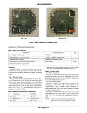
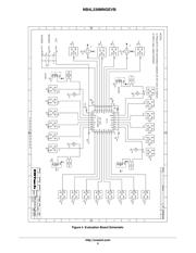
The NB4L339 Evaluation Board was designed to
accommodate a custom QFN−32 socket. Therefore, some
external components were installed on the bottom side of the
board. SMA connectors are provided for all input & output
signal access.
Board Layout
The evaluation board is constructed with FR4 material,
provides a high bandwidth 50 W controlled trace impedance
environment and is designed to minimize noise and
minimize crosstalk.
Layer Stack
L1 Signal
L2 SMA Ground
L3 V
CC
(positive power supply) and V
EE
(Device
negative power supply)
L4 Signal
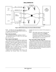
Board Features
• Incorporates on−board slide switches to manually
control CLKSEL, DIVSEL, EN
and MR logic pins,
minimizing cabling
• 2.5 V or 3.3 V single or split−power supply operation
• LVPECL differential output signals are accessed via
SMA connectors
• Convenient and compact board layout
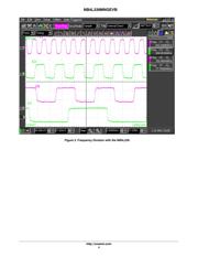
What Measurements Can You Expect to Make?
With this evaluation board, the following measurements
could be performed in single ended or differential modes of
operation.
• Jitter
• Output Skew
• Eye Pattern Generation
• Frequency Performance
• Output Rise and Fall Time
• Phase Noise
http://onsemi.com
EVAL BOARD USER’S MANUAL