
下载
© Semiconductor Components Industries, LLC, 2016
August, 2016 − Rev. 11
1 Publication Order Number:
MC10EP33/D
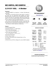
MC10EP33, MC100EP33
3.3V/5V ECL B4 Divider
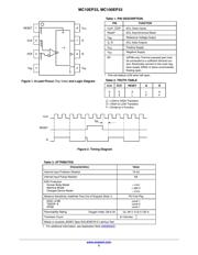
Description
The MC10/100EP33 is an integrated B4 divider. The differential
clock inputs.
The V
BB
pin, an internally generated voltage supply, is available to
this device only. For single-ended input conditions, the unused
differential input is connected to V
BB
as a switching reference voltage.
V
BB
may also rebias AC coupled inputs. When used, decouple V
BB
and V
CC
via a 0.01 mF capacitor and limit current sourcing or sinking
to 0.5 mA. When not used, V
BB
should be left open.
The reset pin is asynchronous and is asserted on the rising edge.
Upon powerup, the internal flip-flops will attain a random state; the
reset allows for the synchronization of multiple EP33’s in a system.
The 100 Series contains temperature compensation.
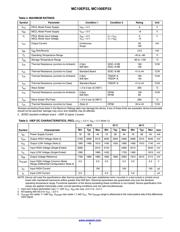
Features
• 320 ps Propagation Delay
• Maximum Frequency = > 4 GHz Typical
• PECL Mode Operating Range:
V
CC
= 3.0 V to 5.5 V with V
EE
= 0 V
• NECL Mode Operating Range:
V
CC
= 0 V with V
EE
= −3.0 V to −5.5 V
• Open Input Default State
• Safety Clamp on Inputs
• Q Output Will Default LOW with Inputs Open or at V
EE
• V
BB
Output
• These Devices are Pb-Free, Halogen Free and are RoHS Compliant
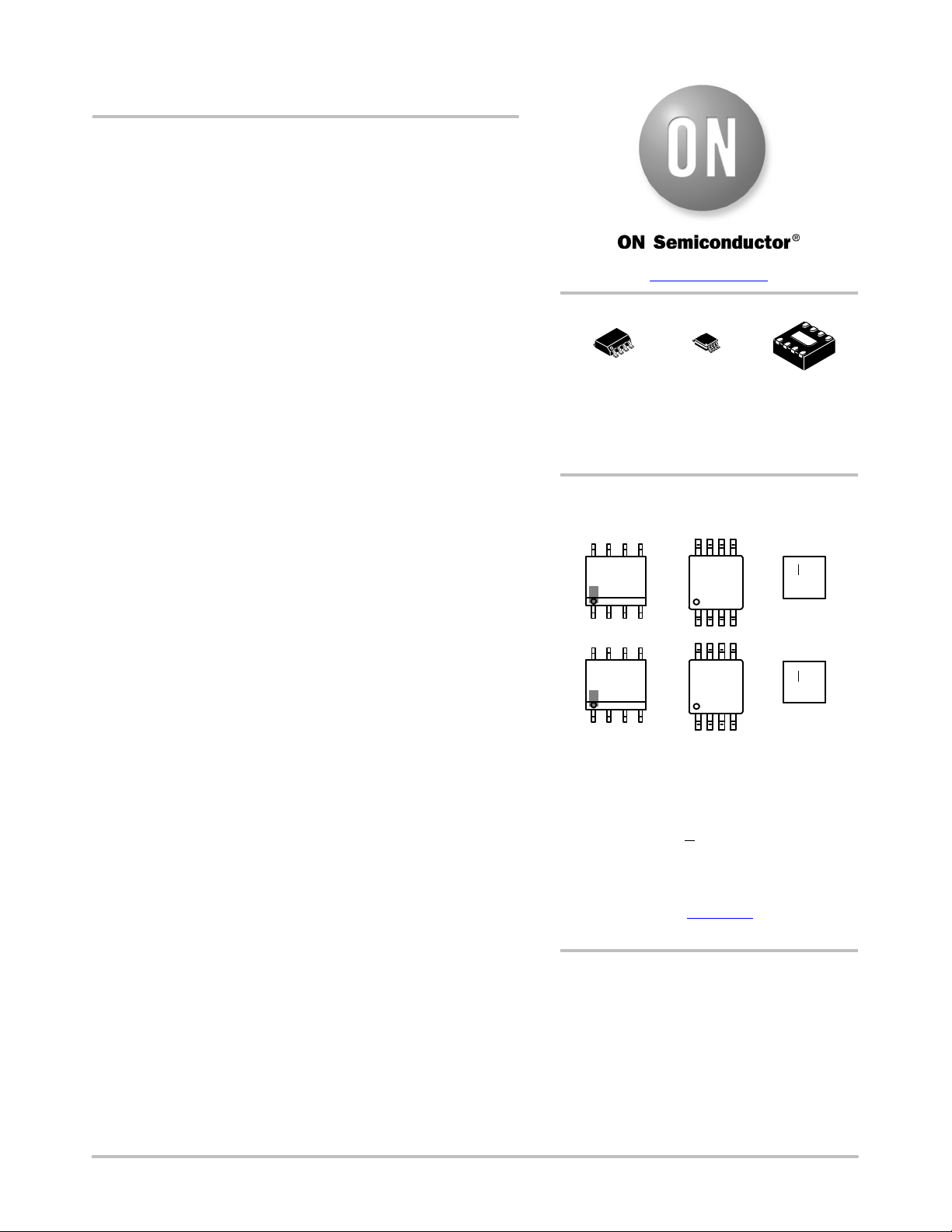
SOIC−8 NB
D SUFFIX
CASE 751−07
MARKING DIAGRAMS*
TSSOP−8
DT SUFFIX
CASE 948R−02
ALYWG
G
HP64
ALYWG
G
KP64
1
8
1
8
1
8
www.onsemi.com
*For additional marking information, refer to
Application Note AND8002/D
.
See detailed ordering and shipping information in the package
dimensions section on page 8 of this data sheet.
ORDERING INFORMATION
1
8
HEP64
ALYW
G
1
8
KEP64
ALYW
G
1
8
DFN8
MN SUFFIX
CASE 506AA
SOIC−8 NB TSSOP−8 DFN8
5Q MG
G
14
3L MG
G
14
H = MC10 A = Assembly Location
K = MC100 L = Wafer Lot
5Q = MC10 Y = Year
3L = MC100 W = Work Week
M
= Date Code
G = Pb-Free Package
(Note: Microdot may be in either location)
页面指南