

下载
© Semiconductor Components Industries, LLC, 2016
August, 2016 − Rev. 7
1 Publication Order Number:
MC100EP16VS/D
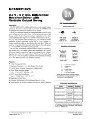
MC100EP16VS
3.3V / 5V ECL Differential
Receiver/Driver with
Variable Output Swing
Description
The MC100EP16VS is a differential receiver with variable output
amplitude. The device is functionally equivalent to the 100EP16 with
an input pin that controls the amplitude of the outputs.
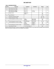
The V
CTRL
input pin controls the output amplitude of the EP16VS
and is referenced to V
CC
. (See Figure 4.) The operational range of the
V
CTRL
input is from ≤ V
BB
(max output amplitude) to V
CC
(min
output amplitude) (See Figure 3). A variable resistor between the V
CC
and V
BB
pins, with the wiper driving V
CTRL
, can control the output
amplitude. Typical application circuits and a V
CTRL
Voltage vs.
Output Amplitude graph are described in this data sheet. When left
open, the V
CTRL
pin will be internally pulled down to V
EE
and operate
as a standard EP16, with 100% output amplitude.
The V
BB
pin, an internally generated voltage supply, is available to
this device only. For Single-Ended input conditions, the unused
differential input is connected to V
BB
as a switching reference voltage.
V
BB
may also rebias AC coupled inputs. When used, decouple V
BB
and V
CC
via a 0.01F capacitor and limit current sourcing or sinking
to 0.5 mA. When not used, V
BB
should be left open.
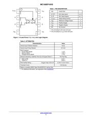
Features
• 220 ps Propagation Delay
• Maximum Frequency = > 4 GHz Typical (See Graph)
• The 100 Series Contains Temperature Compensation
• PECL Mode Operating Range:
V
CC
= 3.0 V to 5.5 V with V
EE
= 0 V
• NECL Mode Operating Range:
V
CC
= 0 V with V
EE
= −3.0 V to −5.5 V
• Open Input Default State
• Q Output Will Default LOW with Inputs Open or at V
EE
• These Devices are Pb-Free, Halogen Free and are RoHS Compliant
A = Assembly Location
L = Wafer Lot
Y = Year
W = Work Week
M = Date Code
G = Pb-Free Package
SOIC−8 NB
D SUFFIX
CASE 751−07
MARKING DIAGRAMS*
TSSOP−8
DT SUFFIX
CASE 948R−02
ALYWG
G
KP62
1
8
1
8
www.onsemi.com
*For additional marking information, refer to
Application Note AND8002/D
.
1
8
KEP62
ALYW
G
1
8
(Note: Microdot may be in either location)
ORDERING INFORMATION
Device Package Shipping†
MC100EP16VSDG SOIC−8 NB
(Pb-Free)
98 Units / Tube
MC100EP16VSDR2G
2500 Tape & Reel
TSSOP−8
(Pb-Free)
MC100EP16VSDTR2G 2500 Tape & Reel
MC100EP16VSDTG 100 Units / Tube
SOIC−8 NB
(Pb-Free)
TSSOP−8
(Pb-Free)
†For information on tape and reel specifications, in-
cluding part orientation and tape sizes, please refer
to our Tape and Reel Packaging Specifications
Brochure, BRD8011/D
.
SOIC−8 NB TSSOP−8
页面指南