

下载
© Semiconductor Components Industries, LLC, 2016
July, 2016 − Rev. 5
1 Publication Order Number:
MC100EL29/D
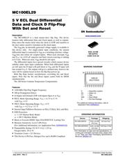
MC100EL29
5 V ECL Dual Differential
Data and Clock D Flip‐Flop
With Set and Reset
Description
The MC100EL29 is a dual master-slave flip flop. The device
features fully differential Data and Clock inputs as well as outputs.
Data enters the master latch when the clock is LOW and transfers to
the slave upon a positive transition on the clock input.
The V
BB
pin, an internally generated voltage supply, is available to
this device only. For single-ended input conditions, the unused
differential input is connected to V
BB
as a switching reference voltage.
V
BB
may also rebias AC coupled inputs. When used, decouple V
BB
and V
CC
via a 0.01 mF capacitor and limit current sourcing or sinking
to 0.5 mA. When not used, V
BB
should be left open.
The differential inputs have special circuitry which ensures device
stability under open input conditions. When both differential inputs
are left open the D input will pull down to V
EE
and the D input will
bias around V
CC
/2. The outputs will go to a defined state, however the
state will be random based on how the flip flop powers up.
Both flip flops feature asynchronous, overriding Set and Reset
inputs. Note that the Set and Reset inputs cannot both be HIGH
simultaneously.
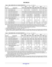
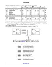
The 100 Series Contains Temperature Compensation.
Features
• 1100 MHz Flip-Flop Toggle Frequency
• 580 ps Propagation Delays
• Q Output will Default LOW with Inputs Open or at V
EE
• PECL Mode Operating Range: V
CC
= 4.2 V to 5.7 V
with V
EE
= 0 V
• NECL Mode Operating Range: V
CC
= 0 V
with V
EE
= −4.2 V to −5.7 V
• Internal Input Pulldown Resistors on D(s), CLK(s), S(s), and R(s).
• ESD Protection:
♦ > 2 kV Human Body Model
♦ > 100 V Machine Model
• Meets or Exceeds JEDEC Spec EIA/JESD78 IC Latchup Test
• Moisture Sensitivity: Level 3 (Pb-Free)
(For Additional Information, see Application Note AND8003/D
)
• Flammability Rating: UL 94 V−0 @ 1.125 in,
Oxygen Index: 28 to 34
• Transistor Count = 313 Devices
• This Device is Pb-Free, Halogen Free and is RoHS Compliant
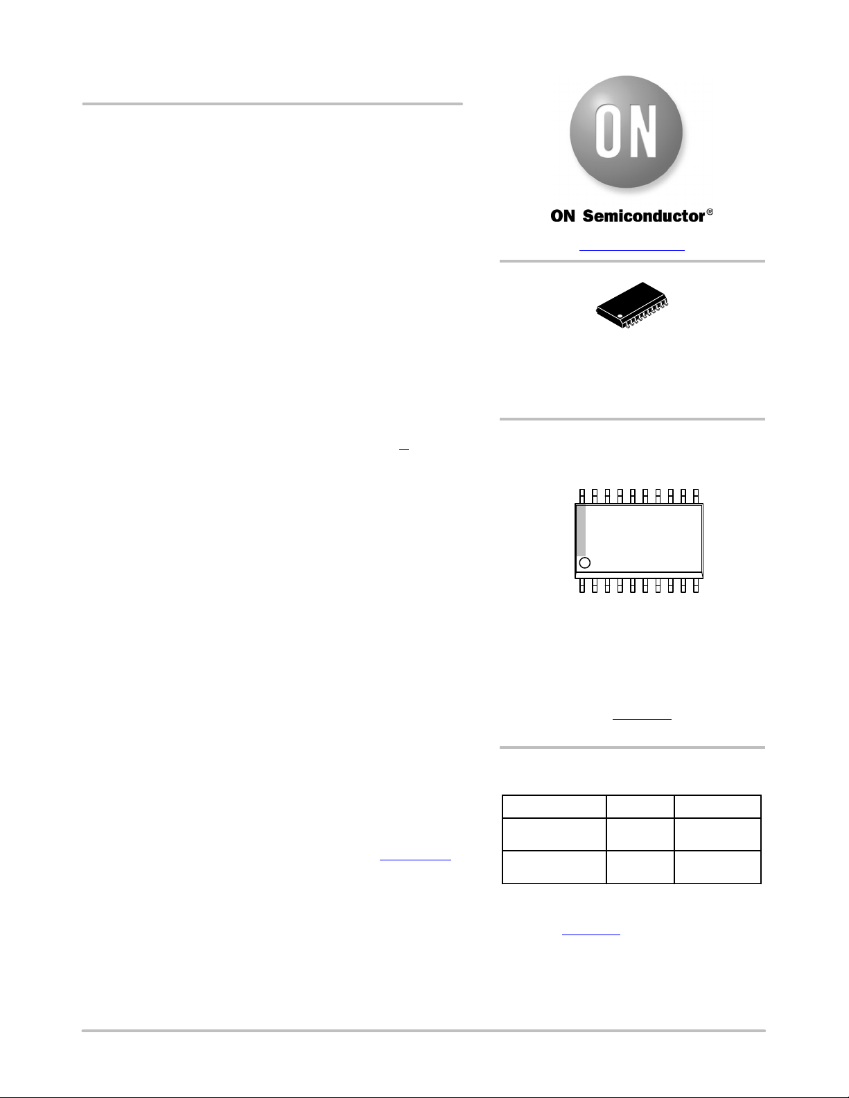
MARKING DIAGRAM*
www.onsemi.com
*For additional marking information, refer to
Application Note AND8002/D
.
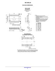
SOIC−20 WB
WB SUFFIX
CASE 751D−05
A = Assembly Location
WL = Wafer Lot
YY = Year
WW = Work Week
G = Pb-Free Package
20
1
100EL29
AWLYYWWG
ORDERING INFORMATION
Device Package Shipping
MC100EL29DWG SOIC−20 WB
(Pb-Free)
38 Units/Tube
MC100EL29DWR2G
1000/Tape & Reel
SOIC−20 WB
(Pb-Free)
†For information on tape and reel specifications, in-
cluding part orientation and tape sizes, please refer
to our Tape and Reel Packaging Specifications
Brochure, BRD8011/D
.
页面指南