

下载
Keywords:
Leaded packages, SMT, PCB design, SOIC, TSSOP, QSOP, SC70, SOT, SOP, QFP
APPLICATION NOTE 6412
SMT ASSEMBLY AND PCB DESIGN GUIDELINES FOR
LEADED PACKAGES
Abstract: This application note provides the PCB design and SMT assembly guidelines for Maxim Integrated’s leaded packages (SOIC,
TSSOP, QSOP, QFP, SC70, SOP, SOT, etc.).
Introduction
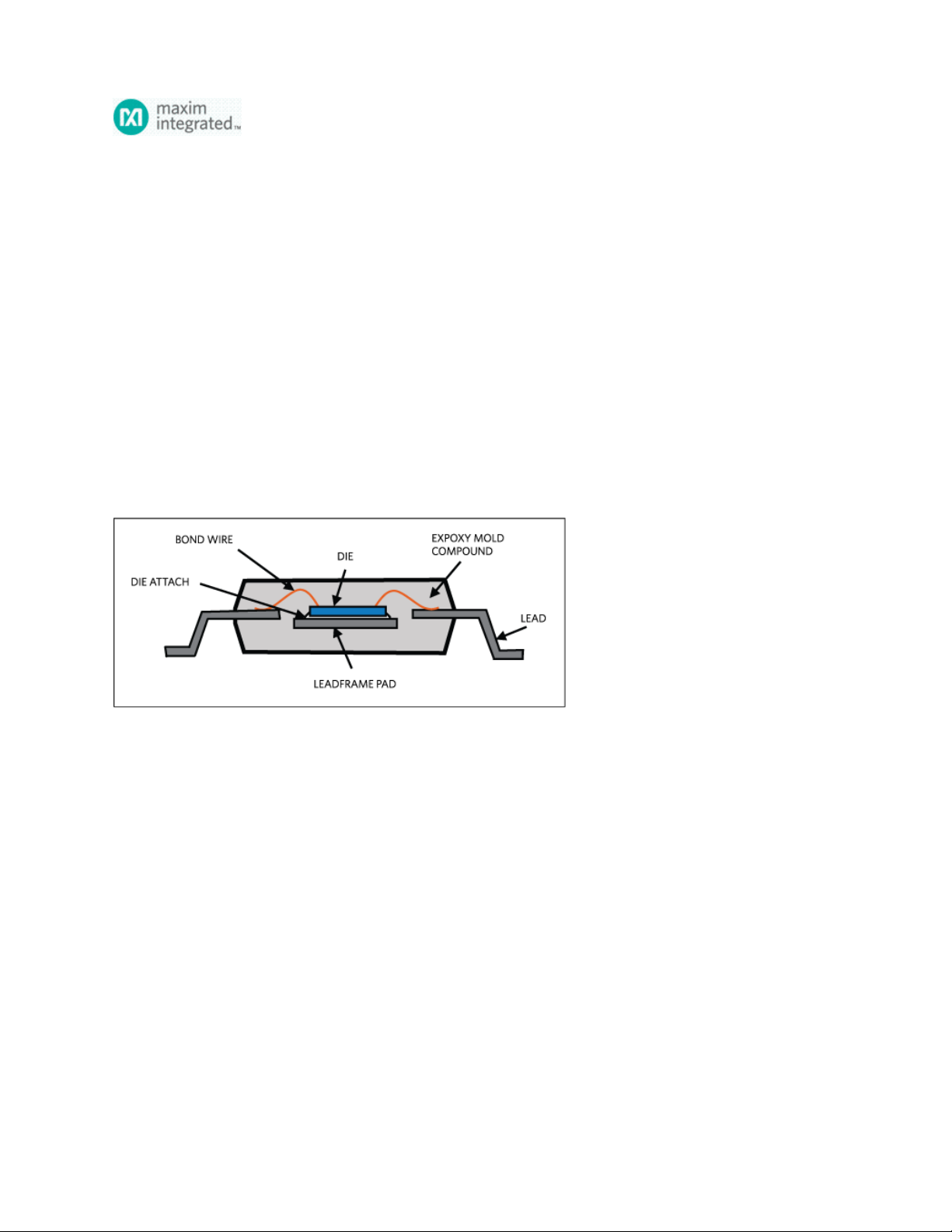
Leaded packages are surface-mount integrated circuit (IC) packages, including such types as quad flat package (QFP), small outline
integrated circuit (SOIC), thin shrink small-outline package (TSSOP), small outline transistor (SOT), SC70, etc. The standard form is a
flat rectangular or square body, with leads extending from two or all four sides. The leads are formed in a gull wing shape to allow solid
footing during assembly to a PCB. Standard Pb-free lead finish is matte tin. Connection is made through the leads of the package,
which can be directly soldered onto the PCB. When an exposed pad is provided in some packages for thermal enhancement purposes,
the exposed pad should be directly soldered onto the PCB.
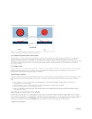
Figure 1 shows the cross-section profile of a leaded package.
Figure 1. Cross-section view of leaded package.
Package Outlines
Package information is available on our website at
www.maximintegrated.com/packages. Users can review package outline drawings
specific to a package type or package code.
PCB Design
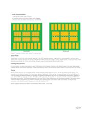
For PCB pad design: a well-designed and manufactured printed circuit board (PCB) is required for optimum manufacturing yields and
product performance. Two types of land patterns are used for surface-mount devices: 1) solder mask-defined (SMD) pads have solder
mask openings that are smaller than metal pads, and 2) nonsolder mask-defined (NSMD) pads have solder mask openings that are
larger than the metal pads. Maxim recommends the use of NSMD pads because they provide a larger metal area for the solder to
anchor to the edges of the metal pads. NSMD improves the solder joint reliability. Only one type of a pad (NSMD or SMD) and one type
of pad surface finish should be used at a given footprint.
Figure 2 illustrates the NSMD and SMD land pattern design.
Land pattern design should follow Maxim’s 90-xxxx series documents corresponding to the specific package code.
Page 1 of 6