

下载
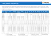
Clock Generator Selector Guide
Product
Independent
Output Freq.
Families
Inputs
Crystal Input
Freq. Range
Xtal Oscillator
or CMOS Input
Freq. Range
Diff Input
Freq. Range
Low-
Jitter
APLLs
Typical
Jitter
fs RMS
NCO
Mode
NCO
ppb
Diff
Outputs
CMOS
Outputs
Output Freq.
Range
NV
Memory
Host
Bus
Supply
Voltage
Pkg
Size,
mm
ZL30236 2 1 XTAL 20 M, 24.576 M 2 700 8 4 1 k–750 M OTP SPI/I2C 3.3 + 1.8 11 × 11
ZL30237 2 1 XTAL 20 M, 24.576 M 2 700
•
0.24 8 4 1 k–750 M OTP SPI/I2C 3.3 + 1.8 11 × 11
ZL30230 4 1 XTAL 20 M, 24.576 M 2 700 4–12 4–12 1 k–750 M OTP SPI/I2C 3.3 + 1.8 11 × 11
MAX24405 2 1 XTAL/SE, 3 D/SE 25 M–52 M 9.72 M–160 M 9.72 M–750 M 2 180
1
0–5 0–10 <1 Hz–750 M Ext EE SPI 3.3 + 1.8 10 × 10
MAX24505 2 1 XTAL/SE, 3 D/SE 25 M–52 M 9.72 M–160 M 9.72 M–750 M 2 180
1
0–5 0–10 <1 Hz–750 M Int EE SPI 3.3 + 1.8 10 × 10
MAX24410 2 1 XTAL/SE, 3 D/SE 25 M–52 M 9.72 M–160 M 9.72 M–750 M 2 180
1
0–10 0–20 <1 Hz–750 M Ext EE SPI 3.3 + 1.8 10 × 10
MAX24510 2 1 XTAL/SE, 3 D/SE 25 M–52 M 9.72 M–160 M 9.72 M–750 M 2 180
1
0–10 0–20 <1 Hz–750 M Int EE SPI 3.3 + 1.8 10 × 10
ZL30250 1 1 XTAL/SE, 3 D/SE 25 M–60 M 9.72 M–300 M 9.72 M–1250 M 1 160
1
•
0.01 0–3 0–6 <1 Hz–1035 M
2
Ext EE
3
SPI/I2C 3.3 + 1.8 5 × 5
ZL30251 1 1 XTAL/SE, 3 D/SE 25 M–60 M 9.72 M–300 M 9.72 M–1250 M 1 160
1
•
0.01 0–3 0–6 <1 Hz–1035 M
2
Int EE
3
SPI/I2C 3.3 + 1.8 5 × 5
ZL30244 2 2 XTAL/SE, 6 D/SE 25 M–60 M 9.72 M–300 M 9.72 M–1250 M 2 160
1
•
0.01 0–6 0–12 <1 Hz–1035 M
2
Ext EE
3
SPI/I2C 3.3 + 1.8 5 × 10
ZL30245 2 2 XTAL/SE, 6 D/SE 25 M–60 M 9.72 M–300 M 9.72 M–1250 M 2 160
1
•
0.01 0–6 0–12 <1 Hz–1035 M
2
Int EE
3
SPI/I2C 3.3 + 1.8 5 × 10
ZL30260 2 1 XTAL/SE, 3D/SE 25 M–60 M 9.72 M–300 M 9.72 M–1250 M 1 170
1
•
0.01 0–6 0–12 1 Hz–1035 M
2
Ext EE
4
SPI/I2C Note
5
8 × 8
ZL30261 2 1 XTAL/SE, 3 D/SE 25 M–60 M 9.72 M–300 M 9.72 M–1250 M 1 170
1
•
0.01 0–6 0–12 1 Hz–1035 M
2
Int EE
4
SPI/I2C Note
5
8 × 8
ZL30262 2 1 XTAL/SE, 3 D/SE 25 M–60 M 9.72 M–300 M 9.72 M–1250 M 1 170
1
•
0.01 0–10 0–20 1 Hz–1035 M
2
Ext EE
4
SPI/I2C Note
5
8 × 8
ZL30263 2 1 XTAL/SE, 3 D/SE 25 M–60 M 9.72 M–300 M 9.72 M–1250 M 1 170
1
•
0.01 0–10 0–20 1 Hz–1035 M
2
Int EE
4
SPI/I2C Note
5
8 × 8
ZL30264 4 1 XTAL/SE, 3 D/SE 25 M–60 M 9.72 M–300 M 9.72 M–1250 M 2 170
1
•
0.01 0–6 0–12 1 Hz–1035 M
2
Ext EE
4
SPI/I2C Note
5
8 × 8
ZL30265 4 1 XTAL/SE, 3 D/SE 25 M–60 M 9.72 M–300 M 9.72 M–1250 M 2 170
1
•
0.01 0–6 0–12 1 Hz–1035 M
2
Int EE
4
SPI/I2C Note
5
8 × 8
ZL30266 4 1 XTAL/SE, 3 D/SE 25 M–60 M 9.72 M–300 M 9.72 M–1250 M 2 170
1
•
0.01 0–10 0–20 1 Hz–1035 M
2
Ext EE
4
SPI/I2C Note
5
8 × 8
ZL30267 4 1 XTALl/SE, 3 D/SE 25 M–60 M 9.72 M–300 M 9.72 M–1250 M 2 170
1
•
0.01 0–10 0–20 1 Hz–1035 M
2
Int EE
4
SPI/I2C Note
5
8 × 8
Abbreviation Key:
D = differential SE = single-ended (CMOS) NCO = numerically controlled oscillator Ext EE = external EEPROM
Int EE = internal EEPROM OTP = one-time programmable 1 = integer-mode APLL-only operation 2 = spread spectrum-capable
3 = up to four configurations (pin-selectable) 4 = up to eight configurations (pin-selectable) 5 = 2.5 V only, 3.3 V only, 1.8 V + 2.5 V, 1.8 V + 3.3 V
Any-Rate Clock Synthesis Devices
Universal clock generators simplify traditional board designs by synthesizing frequencies from either a reference input clock or a common low-cost crystal, providing
low-jitter output clocks. When used together with Microsemi clock distribution fanout buffers, the clock generators provide customers with improved board performance
and complete timing solutions.