
下载

1 About this document
This document provides general hardware and layout
considerations and guidelines for hardware engineers
implementing a DDR4 memory subsystem.
The rules and recommendations in this document serve as an
initial baseline for board designers to begin their specific
implementations, such as fly-by memory topology.
NOTE
It is strongly recommended that the board
designer verifies that all aspects, such as
signal integrity, electrical timings, and so
on, are addressed by using simulation
models before board fabrication.
2
Recommended resources
The following documentation may provide additional,
important information:
• The DDR chapter of the applicable device reference
manual
• Micron’s website: http://www.micron.com
• JEDEC’s website: http://www.jedec.com (a good
example is DDR4 SDRAM Specification)
NXP Semiconductors
Document Number: AN5097
Application Note
Rev. 1, 07/2016
Hardware and Layout Design
Considerations for DDR4 SDRAM
Memory Interfaces
Contents
1 About this document.................................................1
2 Recommended resources.......................................... 1
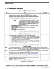
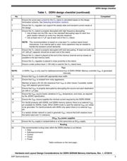
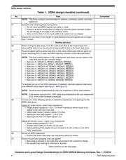
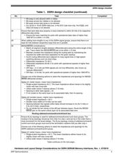
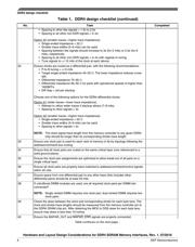
3 DDR4 design checklist................... ..........................2
4 Selecting termination resistors......... ........................ 9
5 Avoiding VREF noise problems........ .......................9
6 Calculating VTT current.................. ........................ 9
7 Layout guidelines for DDR signal
groups..................................................... ................ 10
8 Using simulation models................. .......................15
9 Revision history...................................................... 16
A LS1088A DDR layout routing break
out........................................................................... 17
B DRAM reset signal considerations......................... 23