


下载
User's Guide
SNVA188B–November 2006–Revised April 2013
AN-1531 LP5952 Evaluation Board
1 Introduction
This evaluation board is designed to enable independent evaluation of the LP5952 electrical performance.
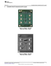
Each board is pre-assembled and tested in the factory.
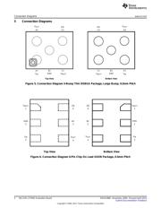
The evaluation kits are available in four output voltage options for the DSBGA package: LP5952TL-1.2EV,
LP5952TL-1.3EV, LP5952TL-1.5EV and LP5952TL-1.8EV and one output voltage option for the COL
USON package: LP5952LC-1.5EV. For other voltage options, the device can be ordered from LP5952
product folder on the TI website.
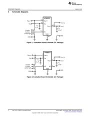
The board contains the LP5952 and input and output capacitors connected to GND.
2 General Description
The LP5952 converts higher input voltages connected to the power input voltage pin V
IN
to lower output
voltages while consuming low quiescent current. The bias input voltage V
BATT
supplies internal circuitry.
The LP5952 is capable of operating with input voltage ranges from 0.7V ≤ V
IN
≤ 4.5V and 2.5V ≤ V
BATT
≤
5.5V for fixed output voltage options from 0.5V to 2.0V. The LP5952 can supply a maximum output current
of 350mA and is particularly suitable for portable, battery-powered systems. It also features internal
protection against short-circuit and over-temperature conditions.
The power input voltage applied between V
IN
and GND should be at least 0.2V above the output voltage
and the bias input voltage applied between V
BATT
and GND should be at least 1.5V above the output
voltage (with a minimum of 2.5V) to operate the device within operating conditions. Input connections
should be kept reasonably short (<20cm) to minimise input inductance and ensure optimum transient
performance.
ON/OFF control of the LP5952 is realized by a logic signal applied to the EN pin. To simplify the enabling
of the device, a three pin jumper is provided on the evaluation board. The middle pin is directly connected
to the EN pin of the device. A logic signal with a minimum of 1.0V to enable the device or with a maximum
of 0.4V to disable the device can be directly connected to this jumper pin in the middle. Alternatively the
middle pin can be shorted to the pin next to it to the left or to the right marked ON or OFF.
A load of up to 350mA maximum may be connected from the V
OUT
pin to GND.
At the bottom of the board the output voltage option (1.2V, 1.3V, 1.5V, or 1.8V) is printed.
The V
OUT_S
pin represents a sense path to the output voltage pin and can be used for more precise voltage
measurements.
All trademarks are the property of their respective owners.
1
SNVA188B–November 2006–Revised April 2013 AN-1531 LP5952 Evaluation Board
Submit Documentation Feedback
Copyright © 2006–2013, Texas Instruments Incorporated