

下载
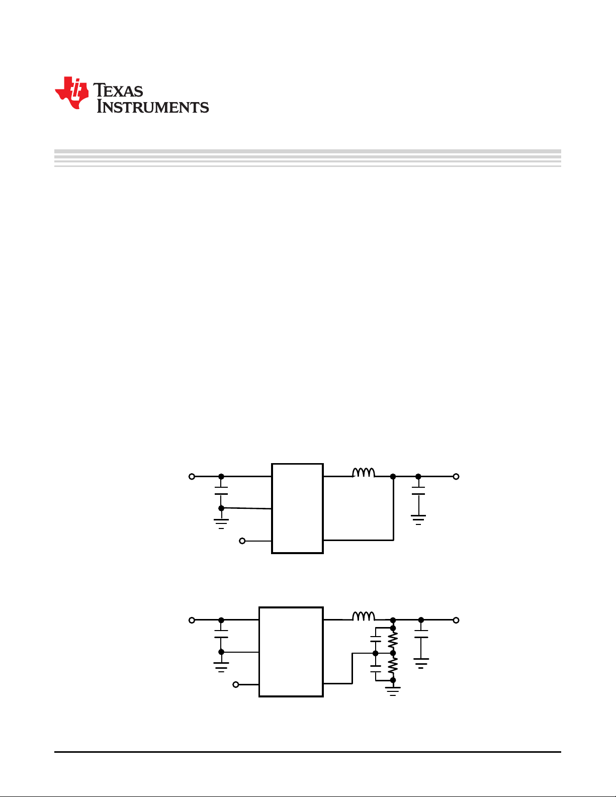
1
2
5
43
V
IN
SW
FB
EN
GND
L1: 2.2 PH
V
OUT
C
OUT
10 PF
C
IN
4.7 PF
LM3674-
ADJ
V
IN
2.7V to 5.5V
R1
R2
C1
C2
1
2
5
43
V
IN
SW
FB
EN
GND
L1: 2.2 PH
V
OUT
C
OUT
10 PF
C
IN
4.7 PF
LM3674
V
IN
2.7V to 5.5V
User's Guide
SNVA139K–January 2006–Revised April 2013
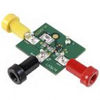
AN-1427 LM3674 Evaluation Board
1 Introduction
The LM3674 evaluation board is a working demonstration of a step down DC-DC converter. This
document contains information about the evaluation board. For further information on buck converter
topology, device electrical characteristics, and component selection, see the device-specific data sheet.
2 General Description
The LM3674 converts high input voltages to lower output voltages with high efficiency through an inductor
based switching topology. The device operates at a fixed-frequency of 2 MHz (typ.) providing high
efficiency during pulse width modulation (PWM) mode. The LM3674 is available in both fixed and
adjustable output voltage options ranging from 1.0 V to 3.3 V in a SOT23-5 package.
3 Operating Conditions
• V
IN
range: 2.7 V ≤ V
IN
≤ 5.5 V
• Recommended load current: 0 mA ≤ I
OUT
≤ 600 mA
• Ambient temperature (T
A
) range: -30°C to +85°C
• Junction temperature (T
J
) range: -30°C to +125°C
4 Typical Application
Figure 1. Typical Application Circuit: Fixed Voltage
Figure 2. Typical Application Circuit: Adjustable Voltage
All trademarks are the property of their respective owners.
1
SNVA139K–January 2006–Revised April 2013 AN-1427 LM3674 Evaluation Board
Submit Documentation Feedback
Copyright © 2006–2013, Texas Instruments Incorporated