
下载

V
OUT
= 2.5V/2A
C
IN
C
OUT
R
FB1
R
FB2
L1
D1
Q1
10 PF
100 PF
10 PH
1k
2.15k
Si2343
LM3475
V
IN
EN
GND
PGATE
FB
1
2
3
4
5
C
FF
1 nF
V
IN
= 5V
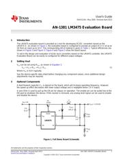
User's Guide
SNVA115A–May 2005–Revised April 2013
AN-1381 LM3475 Evaluation Board
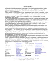
1 Introduction
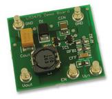
The LM3475 evaluation board is provided as a tool for developing DC/DC converters based on the
LM3475 IC. As shown in Figure 1, the evaluation board is configured to provide an output of 2.5 V at up to
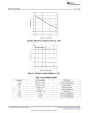
2A from an input up to 10 V. The corresponding bill of material is given in Table 1. Typical efficiencies are
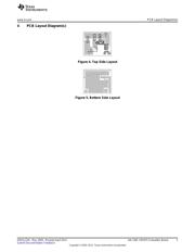
shown in Figure 2 and Figure 3. Figure 4 and Figure 5 show the board layout.
To aid in the design and evaluation of dc/dc buck converters based on the LM3475 controller, the LM3475
Evaluation Board can be easily re-configured for different output voltages.
2 Setting Vout
V
out
can be set using R
FB1
, as shown in Equation 1:
V
OUT
= V
FB
x (R
FB1
+ R
FB2
) / R
FB2
(1)
Where V
FB
is 0.8 V typically.
See the device-specific data sheet before changing any component values, since additional design
adjustments may be required.
3 Optional Components
A feed-forward capacitor C
FF
is placed on the board, which will increase operating frequency. However,
the speed up effect decreases with lower output voltage and is negligible below 1.6 V output.
A zero Ohm is used to pull up the EN pin for always on operation. The enable pin can be pulled low at the
EN post to shutdown the device. If this resistor is removed, any analog level signal can be used to enable
and disable the device.
Figure 1. Full Demo Board Schematic
All trademarks are the property of their respective owners.
1
SNVA115A–May 2005–Revised April 2013 AN-1381 LM3475 Evaluation Board
Submit Documentation Feedback
Copyright © 2005–2013, Texas Instruments Incorporated