

下载
User's Guide
SNVA341A–April 2008–Revised April 2013
AN-1837 LM2738 Evaluation Board
1 Introduction
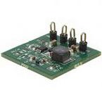
The LM2738 demo board is configured to convert 12V input to 3.3V output at 1.5A load current using the
LM2738X 1.6MHz or the LM2738Y 550kHz step down DC-DC regulator. The tiny low profile MSOP-
PowerPAD-8 and WSON-8 packages allows the demo board to be manufactured using just over one
square inch of a 4-layer printed circuit board.
The circuit is configured with the boost diode connected to V
OUT
, and according to the data sheet, V
OUT
must not exceed the maximum operating limit of 5.5V + V
fD2
using this configuration. This will ensure that
the voltage between the Boost and SW pins, V
BOOST
- V
SW
, does not exceed 5.5V for proper operation.
Please see the LM2738 550kHz/1.6MHz 1.5A Step-Down DC-DC Switching Regulator (SNVS556) data
sheet for more information regarding this requirement.
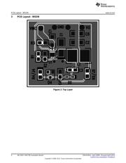
A bill of materials describes the parts used on this demo board. A schematic and layout have also been
included below along with measured performance characteristics. The schematics at the end of this
document show how to re-configure this demo board for various input and output conditions as discussed
in theLM2738 550kHz/1.6MHz 1.5A Step-Down DC-DC Switching Regulator SNVS556 data sheet. Short
or leave open the indicated connection as indicated in the schematics. The above restrictions for the input
voltage are valid only for the demo board as shipped with the demo board schematic (see Figure 1).
2 Operating Conditions
V
IN
= 12V
V
O
= 3.3V
I
O
= 1.5A
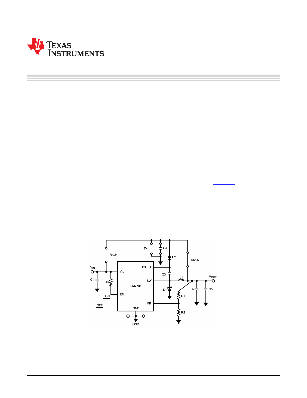
Figure 1. LM2738 Demo Board Schematic - V
BOOST
derived from V
OUT
= 3.3V, V
IN
= 12V
All trademarks are the property of their respective owners.
1
SNVA341A–April 2008–Revised April 2013 AN-1837 LM2738 Evaluation Board
Submit Documentation Feedback
Copyright © 2008–2013, Texas Instruments Incorporated