

下载
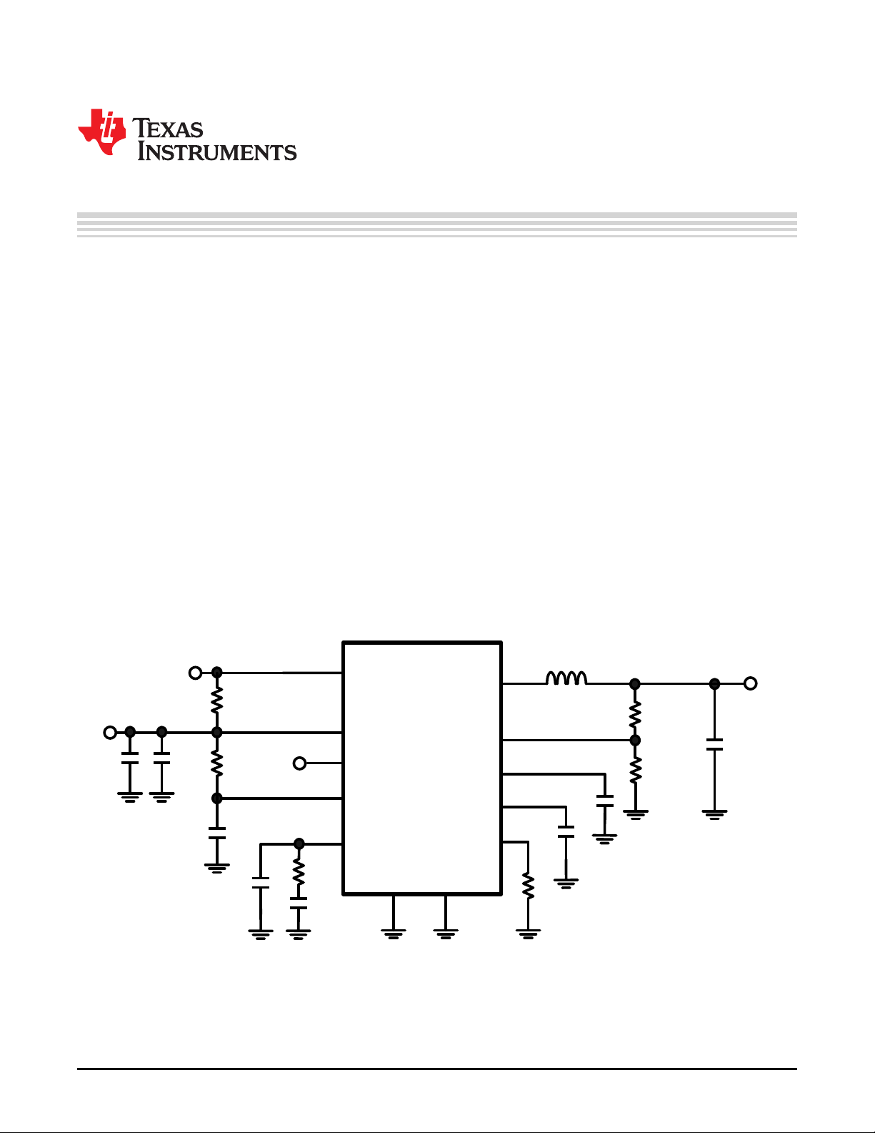
PVIN
SW
AGND
FB
PGOOD
R
FB1
R
FB2
C
OUT
EN
C
SS
SS/TRK
AVIN
C
F
C
C1
COMP
R
C1
V
IN
LM20143
L
R
F
VCC
C
VCC
V
OUT
PGND
P
GOOD
R
PG
EN
C
C2
RT
R
T
C
IN
C
BYP
User's Guide
SNVA277B–October 2007–Revised May 2013
AN-1691 LM20143 Evaluation Board
1 Introduction
The LM20143 is a full featured buck switching regulator capable of driving up to 3A of load current. The
switching frequency of the LM20143 can be varied from 500kHz to 1.5Mhz with an external resistor
allowing the size of the power stage components to be reduced while still providing efficient operation. The
LM20143 is capable of converting an input voltage between 2.95 V and 5.5 V down to an output voltage
as low as 0.8 V. Fault protection features include cycle-by-cycle current limit, output power good, and
output over-voltage protection. The dual function soft-start/tracking pin can be used to control the startup
response of the LM20143, and the precision enable pin can be used to easily sequence the LM20143 in
applications with sequencing requirements. The LM20143 is available in a 16-pin HTSSOP package with
an exposed pad for enhanced thermal performance.
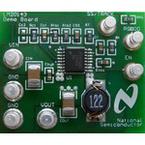
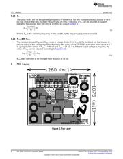
The LM20143 evaluation board has been designed to balance overall solution size with the efficiency of
the regulator. The evaluation board measures just under 1.3” x 1.1” on a two layer PCB, with all
components placed on the top layer. The power stage and compensation components of the LM20143
evaluation board have been optimized for an input voltage of 5 V and a switching frequency of 1.5 MHz,
but for testing purposes, the input can be varied across the entire operating range. The output voltage of
the evaluation board is nominally 1.2 V, but this voltage can be easily changed by replacing one of the
feedback resistors (R
FB1
or R
FB2
). The control loop compensation of the LM20143 evaluation board has
been designed to provide a stable solution over the entire input and output voltage range with a
reasonable transient response. The EN pin must be above 1.18 V (typ) on the board to initiate switching. If
the EN function is not necessary, the EN pin should be externally tied to V
IN
.
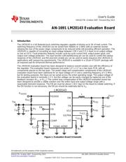
Figure 1. Evaluation Board Schematic
All trademarks are the property of their respective owners.
1
SNVA277B–October 2007–Revised May 2013 AN-1691 LM20143 Evaluation Board
Submit Documentation Feedback
Copyright © 2007–2013, Texas Instruments Incorporated