

下载
1
Application Note 1520
ISL28113/14SOT23EVAL1Z Evaluation Board
User’s Guide
Introduction
The ISL28113/14SOT23EVAL1Z evaluation board is a
design platform containing all the circuitry needed to
characterize critical performance parameters of the
ISL28113 and ISL28114 operational amplifiers, using a
variety of user defined test circuits.
The ISL28113 and ISL28114 CMOS operational
amplifiers feature low power consumption, low input bias
current, and rail-to-rail input and output drive capability.
They are designed to operate with a single lithium cell or
two Ni_Cd batteries.
Reference Documents
• ISL28113 Data Sheet, FN6728
• ISL28114 Data Sheet, FN6800
Evaluation Board Key Features
The ISL28113/14SOT23EVAL1Z is designed to enable the
IC to operate from a single supply, +2.4VDC to +5.5VDC
or from split supplies, ±1.2VDC to ±2.75V. The board is
configured for a single op amp connected for differential
input with a closed loop gain of 10. A single external
reference voltage (VREF) pin and provisions for a user-
selectable voltage divider - filter are included.
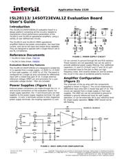
Power Supplies (Figure 1)
External power connections are made through the +V, -V
and Ground connections on the evaluation board. For
single supply operation, the -V and Ground pins are tied
together to the power supply negative terminal. For split
supplies, +V and -V terminals connect to their respective
power supply terminals. De-coupling capacitors C2 and
C4 can connect to ground through R4 and R16 resistors.
These resistors are not populated, but can be used to
provide additional power supply filtering. Four additional
capacitors, C1 and C5 (0.01µF) and C7 and C8 (0.1µF)
are connected close to the part to filter out high
frequency noise. Anti-reverse diodes D1 and D2 protect
the circuit in the case of accidental polarity reversal.
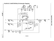
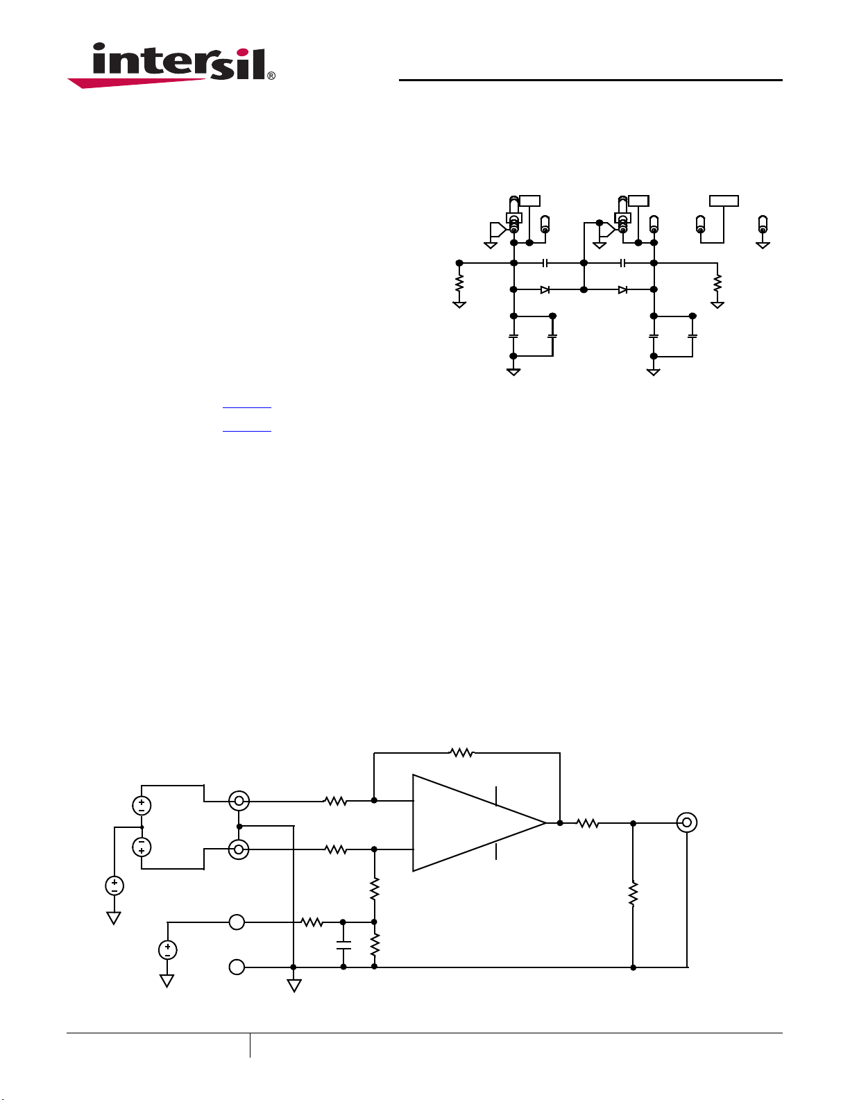
Amplifier Configuration
(Figure 2)
The schematic of the op-amp with the components
supplied is shown in Figure 2. The circuit implements a
differential input amp with a closed loop gain of 10. The
circuit can operate from a single supply or from dual
supplies. The VREF pin can be connected to ground to
establish a ground referenced input for split supply
operation, or can be externally set to any reference level
for single supply operation. Note: VREF should not be
left floating.
R4
D2D1
R16
C2 C4
J8
J11
J9
J10
J7
J13
DNP
DNP
S1AB
4.7µF 4.7µF
S1AB
VREF
V+V-
0.1µF
C7
C1
0.01µF
0.1µF
C8
C5
0.01µF
FIGURE 1. POWER SUPPLY CIRCUIT
IN-
IN+
RF
VREF
IN -
IN +
GND
100k
RREF+
10k
VOUT
ISL28113, ISL28114
VP
V-
0Ω
VM
VCM
IN-
IN+
VREF
V+
RIN-
10k
RIN+
10k
-
+
0Ω
100k
RL
10k
FIGURE 2. BASIC AMPLIFIER CONFIGURATION
CAUTION: These devices are sensitive to electrostatic discharge; follow proper IC Handling Procedures.
1-888-INTERSIL or 1-888-468-3774
| Intersil (and design) is a registered trademark of Intersil Americas Inc.
Copyright Intersil Americas Inc. 2010. All Rights Reserved
All other trademarks mentioned are the property of their respective owners.
January 19, 2010
AN1520.0