


下载
EK1HMC7043LP7F User Guide
UG-892
One Technology Way • P. O. Box 9106 • Norwood, MA 02062-9106, U.S.A. • Tel: 781.329.4700 • Fax: 781.461.3113 • www.analog.com
Evaluating the HMC7043 High Performance, 3.2 GHz, 14-Output Fanout Buffer
PLEASE SEE THE LAST PAGE FOR AN IMPORTANT
WARNING AND LEGAL TERMS AND CONDITIONS.
Rev. 0 | Page 1 of 9
FEATURES
Simple power connection using USB connection and
on-board low dropout (LDO) voltage regulator
LDO can be bypassed for power measurements
AC-coupled differential SMA connectors
SMA connectors for
1 clock input
1 RF sync input
6 clock outputs
Microsoft® Windows®–based evaluation software with
simple graphical user interface (GUI)
Easy access to digital input/output and diagnostic signals via
input/output header (GPIO)
Status LED for diagnostic signals
USB computer interface
EVALUATION KIT CONTENTS
EV2HMC7043LP7F evaluation board
USB interface board and USB cable
EK1HMC7043LP7F user guide
GENERAL DESCRIPTION
This user guide describe the hardware and software of the
HMC7043 evaluation kit. The evaluation board schematics and
printed circuit board (PCB) layout artwork can be found on the
HMC7043 evaluation kit page.
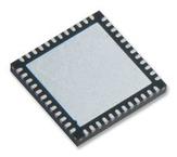
The HMC7043 is a high performance clock buffer for the
distribution of ultralow phase noise references for high speed
data converters with either parallel or serial (JESD204B type)
interfaces. The HMC7043 is designed to meet the requirements
of multicarrier GSM and LTE base station designs, and offers a
wide range of clock management and distribution features to
simplify baseband and radio card clock tree designs.
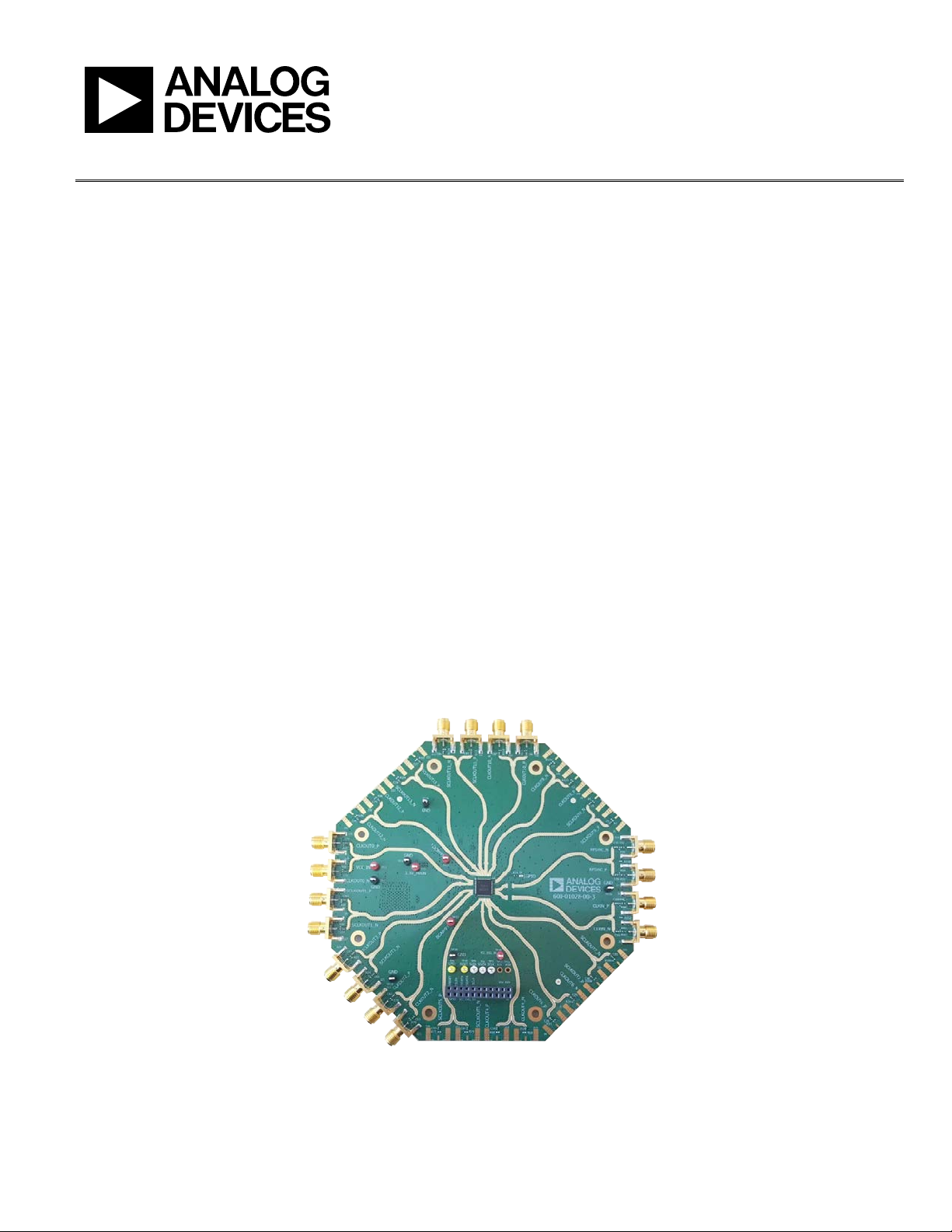
The EK1HMC7043LP7F evaluation kit is a compact, easy-to-use
platform for evaluating all the features of the HMC7043. All
inputs and outputs are configured as differential on the
EV2HMC7043LP7F evaluation board.
Full specifications on the HMC7043 are available in the product
data sheet, which should be consulted in conjunction with this
user guide when working with the evaluation board.
EVALUATION BOARD PHOTOGRAPH
13687-001
Figure 1.