

下载

SGUS056A − MARCH 2005 − REVISED FEBRUARY 2006
1
POST OFFICE BOX 655303 • DALLAS, TEXAS 75265
Controlled Baseline
− One Assembly/Test Site, One Fabrication
Site
Extended Temperature Performance of up
to −40°C to 105°C
Enhanced Diminishing Manufacturing
Sources (DMS) Support
Enhanced Product-Change Notification
Qualification Pedigree
†
Highest-Performance Fixed-Point DSPs
− 1.67-/1.39-/1.17-/1-ns Instruction Cycle
− 600-/720-/850-MHz, 1-GHz Clock Rate
− Eight 32-Bit Instructions/Cycle
− Twenty-Eight Operations/Cycle
− 4800, 5760, 6800, 8000 MIPS
− Fully Software-Compatible With C62x
− C6414/15/16 Devices Pin-Compatible
VelociTI.2 Extensions to VelociTI
Advanced Very-Long-Instruction-Word
(VLIW) TMS320C64x DSP Core
− Eight Highly Independent Functional
Units With VelociTI.2 Extensions
− Non-Aligned Load-Store Architecture
− 64 32-Bit General-Purpose Registers
− Instruction Packing Reduces Code Size
− All Instructions Conditional
VCP
− Supports Over 833 7.95-Kbps AMR
− Programmable Code Parameters
TCP
− Supports up to 10 2-Mbps or
60 384-Kbps 3GPP (6 Iterations)
− Programmable Turbo Code and
Decoding Parameters
L1/L2 Memory Architecture
− 128K-Bit (16K-Byte) L1P Program Cache
(Direct Mapped)
− 128K-Bit (16K-Byte) L1D Data Cache
(2-Way Set-Associative)
− 8M-Bit (1024K-Byte) L2 Unified Mapped
RAM/Cache (Flexible Allocation)
Two External Memory Interfaces (EMIFs)
− One 64-Bit (EMIFA), One 16-Bit (EMIFB)
− Glueless Interface to Asynchronous
Memories and Synchronous Memories
− 1280M-Byte Total Addressable External
Memory Space
Instruction Set Features
− Byte-Addressable (8-/16-/32-/64-Bit Data)
− 8-Bit Overflow Protection
− Bit-Field Extract, Set, Clear
− Normalization, Saturation, Bit-Counting
− VelociTI.2 Increased Orthogonality
Enhanced Direct-Memory-Access (EDMA)
Controller (64 Independent Channels)
Host-Port Interface (HPI)
− User-Configurable Bus Width (32-/16-Bit)
32-Bit/33-MHz, 3.3-V PCI Master/Slave
Interface Conforms to PCI Specification 2.2
− Three PCI Bus Address Registers
− Four-Wire Serial EEPROM Interface
− PCI Interrupt Request Under DSP
Program Control
− DSP Interrupt Via PCI I/O Cycle
Three Multichannel Buffered Serial Ports
− Direct Interface to T1/E1, MVIP, SCSA
Framers
− Up to 256 Channels Each
− ST-Bus-Switching-, AC97-Compatible
− Serial Peripheral Interface (SPI)
Compatible (Motorola)
Three 32-Bit General-Purpose Timers
UTOPIA [C6416T]
− UTOPIA Level 2 Slave ATM Controller
− 8-Bit Transmit and Receive Operations
up to 50 MHz per Direction
− User-Defined Cell Format up to 64 Bytes
16 General-Purpose I/O (GPIO) Pins
IEEE-1149.1 (JTAG
‡
)
Boundary-Scan-Compatible
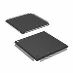
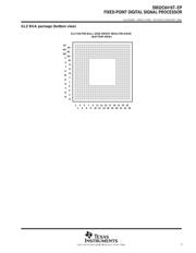
532-Pin Ball Grid Array (BGA) Package
(GLZ Suffix), 0,8-mm Ball Pitch
Please be aware that an important notice concerning availability, standard warranty, and use in critical applications o
f
Texas Instruments semiconductor products and disclaimers thereto appears at the end of this data sheet.
!"# "#$" "%&$#" " '&# " &! #$" "! '$!
% !(!)'!"#* ! #$# % !$ !(! "$#! " #! '$+!,-
'!%."+ # !)!#&$) $&$#!&#*
Copyright 2006, Texas Instruments Incorporated
C62x, VelociTI.2, VelociTI, and TMS320C64x are trademarks of Texas Instruments.
Motorola is a trademark of Motorola, Inc.
†
Component qualification in accordance with JEDEC and industry standards to ensure reliable operation over an extended temperature range.
This includes, but is not limited to, Highly Accelerated Stress Test (HAST) or biased 85/85, temperature cycle, autoclave or unbiased HAST,
electromigration, bond intermetallic life, and mold compound life. Such qualification testing should not be viewed as justifying use of this
component beyond specified performance and environmental limits.
‡
IEEE Standard 1149.1-1990 Standard-Test-Access Port and Boundary Scan Architecture.