
下载

Altera Virtual JTAG (altera_virtual_jtag) IP Core User
Guide
2015.11.20
UG-SLDVRTL
Subscribe
Send Feedback
The Altera Virtual JTAG (altera_virtual_jtag) megafunction IP core provides access to the PLD source
through the JTAG interface. This IP core is optimized for Altera device architectures. Using IP cores in
place of coding your own logic saves valuable design time, and offers more efficient logic synthesis and
device implementation. You can scale the IP core's size by setting parameters.
Related Information
Introduction to Altera IP Cores
Introduction
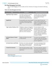
The Virtual JTAG IP core allows you to create your own software solution for monitoring, updating, and
debugging designs through the JTAG port without using I/O pins on the device, and is one feature in the
On-Chip Debugging Tool Suite. The Quartus
®
II software or JTAG control host identifies each instance of
this IP core by a unique index. Each IP core instance functions in a flow that resembles the JTAG
operation of a device. The logic that uses this interface must maintain the continuity of the JTAG chain on
behalf the PLD device when this instance becomes active.
With the Virtual JTAG IP core you can build your design for efficient, fast, and productive debugging
solutions. Debugging solutions can be part of an evaluation test where you use other logic analyzers to
debug your design, or as part of a production test where you do not have a host running an embedded
logic analyzer. In addition to debugging features, you can use the Virtual JTAG IP core to provide a single
channel or multiple serial channels through the JTAG port of the device. You can use serial channels in
applications to capture data or to force data to various parts of your logic.
Each feature in the On-Chip Debugging Tool Suite leverages on-chip resources to achieve real time
visibility to the logic under test. During runtime, each tool shares the JTAG connection to transmit
collected test data to the Quartus II software for analysis. The tool set consists of a set of GUIs, IP core
intellectual property (IP) cores, and Tcl application programming interfaces (APIs). The GUIs provide the
configuration of test signals and the visualization of data captured during debugging. The Tcl scripting
interface provides automation during runtime.
The Virtual JTAG IP core provides you direct access to the JTAG control signals routed to the FPGA core
logic, which gives you a fine granularity of control over the JTAG resource and opens up the JTAG
resource as a general-purpose serial communication interface. A complete Tcl API is available for sending
and receiving transactions into your device during runtime. Because the JTAG pins are readily accessible
©
2015 Altera Corporation. All rights reserved. ALTERA, ARRIA, CYCLONE, ENPIRION, MAX, MEGACORE, NIOS, QUARTUS and STRATIX words and logos are
trademarks of Altera Corporation and registered in the U.S. Patent and Trademark Office and in other countries. All other words and logos identified as
trademarks or service marks are the property of their respective holders as described at www.altera.com/common/legal.html. Altera warrants performance
of its semiconductor products to current specifications in accordance with Altera's standard warranty, but reserves the right to make changes to any
products and services at any time without notice. Altera assumes no responsibility or liability arising out of the application or use of any information,
product, or service described herein except as expressly agreed to in writing by Altera. Altera customers are advised to obtain the latest version of device
specifications before relying on any published information and before placing orders for products or services.
ISO
9001:2008
Registered
www.altera.com
101 Innovation Drive, San Jose, CA 95134