
下载
1
dc1789afa
DEMO MANUAL DC1789A
Description
LTM2884
Isolated USB Transceiver
with Isolated Power
Demonstration circuit 1789A is an isolated USB transceiver
with isolated power featuring the LT M
®
2884. The demo
circuit features an EMI optimized circuit configuration and
printed circuit board layout. All components are integrated
into the µModule
®
isolator. The demo circuit operates
from a supply on V
CC
and/or V
BUS
. The part generates
an isolated output voltage on V
CC2
and communicates all
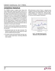
performance summary
operating principles
necessary signaling across the isolation barrier through
LTC’s isolator µModule technology.
Design files for this circuit board are available at
http://www.linear.com/demo
L, LT, LTC, LTM, Linear Technology, the Linear logo and µModule are registered trademarks of
Linear Technology Corporation. All other trademarks are the property of their respective owners.
(T
A
= 25°C)
The LTM2884 contains an isolated DC/DC converter de-
livering power to V
CC2
at 5V from the input supply V
CC
and/or V
BUS
. Isolation is maintained by the separation of
GND and GND2 where significant operating voltages and
transients can exist without affecting the operation of the
LTM2884. The logic side ON pin enables or shuts down
the LTM2884. All logic side signals are referenced to the
logic supply pin V
LO
. The LTM2884 has two power supply
inputs, V
CC
and V
BUS
. For applications requiring more
than 200mA from V
CC2
, V
CC
must be connected to an
external supply of 8.1V to 16.5V. V
BUS
may be connected
SYMBOL PARAMETER CONDITIONS MIN TYP MAX UNITS
V
CC
Operating Supply Range (Isolated Power Input) 4.4 12 16.5 V
V
BUS
Operating Supply Range (USB Bus Power Input) 4.4 5 16.5 V
V
CC2
Regulated Output Voltage V
CC
= V
BUS
= 4.4V, I
CC2
= 200mA
V
CC
= 8.1V, I
CC2
= 500mA
4.75
4.75
5
5
5.25
5.25
V
V
t
LDR
Low Speed Data Rate 1.5 Mbps
t
FDR
Full Speed Data Rate 12 Mbps
V
IORM
Maximum Working Insulation Voltage GND to GND2 560
400
V
DC
V
RMS
Common Mode Transient Immunity 30 kV/µs
to USB bus power or to the external supply. For applica-
tions requiring 200mA or less connect V
CC
and V
BUS
to
USB bus power.
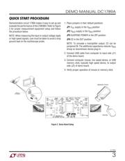
Upstream USB signaling is controlled by the bidirectional
pins D1
+
and D1
–
. A 1.5k pull-up resistor is automatically
configured dependent upon the connected downstream
peripheral device. For full speed and low speed devices
the pull-up is asserted on D1
+
and D1
–
, respectively. The
downstream USB data pins, D2
+
and D2
–
, each have
integrated 15k pull-down resistors.