

下载
1
features
D
Function, Pinout, Speed, and Drive
Compatible With F Logic
D
All Products Capable of Live Insertion
D
All Products Meet FCT Logic JEDEC
Standard No. 8A
D
Edge-Rate Control Circuitry for
Significantly Improved Noise
Characteristics
D
Power-Off Disable Feature on All Families
D
Matched Output Signal Rise and Fall Times
D
CMOS for Low Power Consumption:
Typically 1/3 of the Fastest Advanced
Schottky TTL Logic
D
Inputs and Outputs Interface Directly With
TTL, NMOS, and CMOS Devices
D
Typically 64-mA Sink and 32-mA Source
Drive Capability
D
3-State Outputs on Most Devices
D
Operational Over the Full Commercial and
Military Temperature Ranges (Octal)
D
Industrial Temperature Range of –40
_
C to
85
_
C (16-Bit Family)
D
Products Available to Latest Revision of
MIL-STD-833 Class B Compliance
functional description
introduction
The CYxxFCT-T logic families acquired from Cypress offer the lowest power solution for the design of
high-speed systems. All logic families are TTL compatible, which means that they conform to the
industry-standard TTL voltage levels and TTL threshold point of 1.5 V. All inputs have hysteresis. The benefit
to the user is increased static and dynamic noise immunity, as well as less sensitivity to noise superimposed
on slowly rising or falling inputs.
the original FCT
The outputs of the original (non-Cypress) FCT family swung rail-to-rail, i.e., from V
OL
= 0.4 V to
V
OH
= V
CC
– 0.2 V. The data sheets specify V
OH
minimum as 2.4 V when sourcing 15 mA and typical as 4.3 V.
The output pullup transistor is a p-channel device. Typical unloaded output signal rise and fall times are 1 ns.
CYxxFCT-T from Cypress
The new, 5-V V
CC
CYxxFCT-T logic families feature output buffers that use n-channel pullup transistors and
controlled rise- and fall-time edge rates. Typical unloaded output signal rise and fall times are 1 ns. The
maximum unloaded output high voltage, V
OH
, is V
CC
minus the n-channel threshold, V
T
. The transistor drain
is connected to V
CC
, so V
T
is approximately 1 V. The loaded V
OH
typically is 3.3 V when sourcing 15 mA with
a V
CC
of 5 V.
The reduced output voltage swing of CYxxFCT-T results in lower crosstalk. The controlled edge rates reduce
crosstalk, as well as ground bounce and, in addition, reduce output signal overshoot and undershoot.
These products have no diodes from input pins, output pins, or I/O pins to V
CC
. This means that they all are
capable of being inserted or withdrawn from operating systems without turning off the power.
These logic families produced by Cypress operate from a 5-V power source. The products consist of octals (8-bit
data path), either with high-drive (source 32 mA/sink 64 mA) or 25-Ω (output) series resistors, and 16-bit-wide
data-path products, either with high-drive or balanced-drive (24-mA source/sink) outputs. Some of these
products have bus-hold inputs.
Copyright 2001, Texas Instruments Incorporated
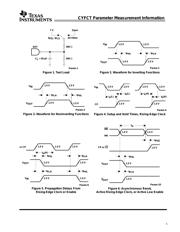
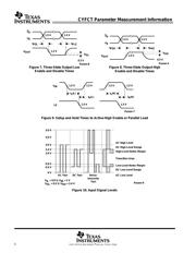
CYFCT Parameter Measurement Information
SCCU001 – APRIL 2001