
下载
Atmel-8826B-SEEPROM-PCB-Mounting-Guidelines-Surface-Mount-Packages-ApplicationNote_042016
Introduction
This document provides PCB designers with a set of guidelines for successful
board mounting of Atmel
®
surface mount packages. Package Land Pattern
descriptions are depicted by the package family, and although each family is
represented by a single body size and lead count, the individual land description
apply to all packages within a particular family. Land Pattern descriptions were
provided by IPC-7351 Calculator from the Mentor Graphics Corporation. These
are only general guidelines that Atmel received from the IPC-7351 Calculator. The
solder reflow guidelines are derived from IPC -9502. Atmel does not make direct
recommendation for board design, nor does it take legal liability and responsibility
for the information in this document. Please refer to the IPC website for more
information regarding board design and processing.
1. Solder Reflow Process
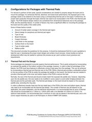
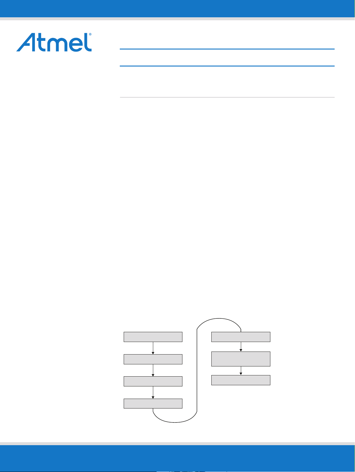
Figure 1-1 shows the typical process flow for mounting surface mount packages
to printed circuit boards. It is important to include the post print and the post reflow
inspection, especially during the process development. The volume of paste
printed should be measured either by 2D or 3D techniques. The paste volume
should be around 80% to 90% of the stencil aperture volume to indicate a good
paste release. After reflow, the mounted package should be inspected by
transmission x-ray for the presence of voids, solder balling, or other defects.
Cross-sectioning may also be required to determine the fillet shape, size, and the
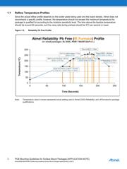
joint standoff height during process development. A typical reflow profile for
no-clean solder paste is shown in Figure 1-2, temperature measured at the solder
joint.
Figure 1-1. Typical PCB Mounting Process Flow
Solder Paste Printing
Component Placement
Pre-Reflow Inspection
Reflow
Post Reflow Inspection
(Visual/X-ray)
Rework and Touch-up
Post Print Inspection
APPLICATION NOTE
PCB Mounting Guidelines for Surface Mount Packages