
下载
User's Guide
SLAU160 – July 2005
ADS8372EVM
This user's guide describes the characteristics, operation, and use of the ADS8372
16-bit, 600 kHz, high speed, serial interface Analog-to-Digital converter Evaluation
Board (EVM). A complete circuit description, schematic diagram, and bill of materials
are included.
The following related documents are available on the TI web site at www.ti.com .
Data Sheets: Literature Numbers:
ADS8372 SLAS451
REF1004C-2.5 SBVS002
SN74AHC1G125 SCLS377
THS4131 SLOS318
OPA627AU SBOS165
Contents
1 EVM Overview ............................................................................................................... 2
2 Analog Interface .............................................................................................................. 2
3 Digital Interface .............................................................................................................. 4
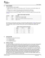
4 Power Supplies .............................................................................................................. 5
5 Using the EVM ............................................................................................................... 5
6 ADS8372EVM Bill Of Materials ............................................................................................ 7
8 Board Layers ................................................................................................................. 9
9 Schematics .................................................................................................................. 11
List of Figures
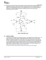
1 Input Buffer Circuit ........................................................................................................... 3
2 Top Layer ..................................................................................................................... 9
3 Power Plane .................................................................................................................. 9
4 Ground Plane ............................................................................................................... 10
5 Bottom Layer ................................................................................................................ 10
List of Tables
1 Analog Input Connector ..................................................................................................... 2
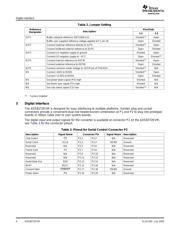
2 Jumper Setting ............................................................................................................... 4
3 Pinout for Serial Control Connector P2 ................................................................................... 4
4 Power Supply Test Points .................................................................................................. 5
5 Power Connector (J3) Pin Out ............................................................................................. 5
7 ADS8372EVM Bill of Materials ............................................................................................. 7
SLAU160 – July 2005 ADS8372EVM 1