


下载
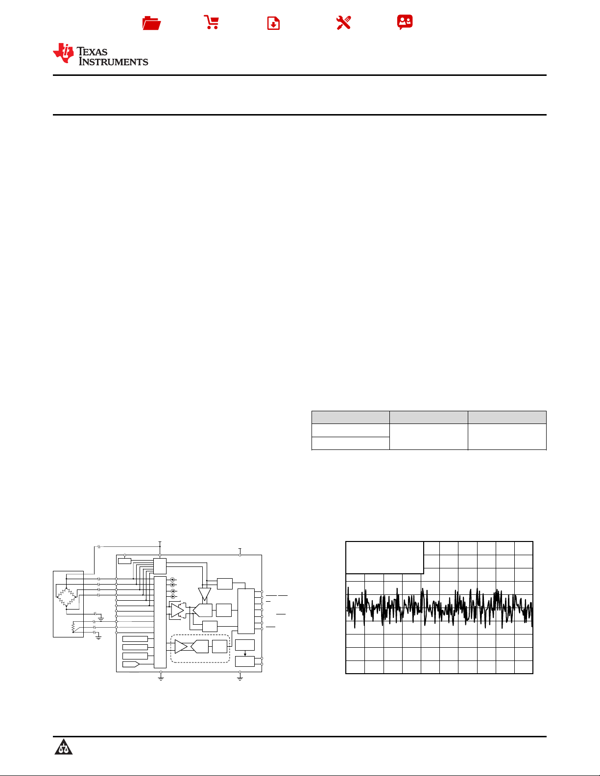
Time (s)
ADC Output (PV)
0 1 2 3 4 5 6 7 8 9 10
-0.25
-0.2
-0.15
-0.1
-0.05
0
0.05
0.1
0.15
0.2
0.25
D017
Input Range = r78 mV
Data Rate = 20 SPS
Noise = 0.16 PV
P-P
32-Bit
ûADC
PGA
Input
Mux
Digital
Filter
Serial
Interface
and
Control
CS
DOUT/DRDY
SCLK
DRDY
START
Clock
Mux
XTAL2
XTAL1/CLKIN
REFOUT
Ref
Alarm
Signal
Alarm
Buf
AIN0
AIN1
AIN2
AINCOM
GPIO
Level Shift
Temp Sensor
ADS1262
ADS1263
+5 V
DVDD
DGND
Ref
Mux
2.5-V Ref
AIN3
AIN4
AIN5
AIN6
AIN7
AIN8
AIN9
PGA
ADS1263 Only
Digital
Filter
Dual Sensor
Excitation
Test V
Internal
Oscillator
24-Bit
ûADC
RESET/PWDN
DIN
AVSS
AVDD
+Exc
±Exc
±Sig
+Sig
±Sen
+Sen
Sensor Test
PGA
Pt 100
Bridge
+3.3 V
Product
Folder
Sample &
Buy
Technical
Documents
Tools &
Software
Support &
Community
ADS1262
,
ADS1263
SBAS661B –FEBRUARY 2015–REVISED JULY 2015
ADS126x 32-Bit, Precision, 38-kSPS, Analog-to-Digital Converter (ADC)
with Programmable Gain Amplifier (PGA) and Voltage Reference
1 Features 3 Description
The ADS1262 and ADS1263 are low-noise, low-drift,
1
• Precision, 32-bit, ΔΣ ADC
38.4-kSPS, delta-sigma (ΔΣ) ADCs with an integrated
• Auxiliary 24-Bit, ΔΣ ADC (ADS1263)
PGA, reference, and internal fault monitors. The
• Data Rates: 2.5 SPS to 38400 SPS
ADS1263 integrates an auxiliary, 24-bit, ΔΣ ADC
intended for background measurements. The sensor-
• Differential Input, CMOS PGA
ready ADCs provide complete, high-accuracy, one-
• 11 Multifunction Analog Inputs
chip measurement solutions for the most-demanding
• High-Accuracy Architecture
sensor applications, including weigh scales, strain-
gauge sensors, thermocouples, and resistance
– Offset Drift: 1 nV/°C
temperature devices (RTD).
– Gain Drift: 0.5 ppm/°C
The ADCs are comprised of a low-noise, CMOS PGA
– Noise: 7 nV
RMS
(2.5 SPS, Gain = 32)
(gains 1 to 32), a ΔΣ modulator, followed by a
– Linearity: 3 ppm
programmable digital filter. The flexible analog front-
• 2.5-V Internal Voltage Reference
end (AFE) incorporates two sensor-excitation current
sources suitable for direct RTD measurement.
– Temperature Drift: 2 ppm/°C
• 50-Hz and 60-Hz Rejection
A single-cycle settling digital filter maximizes multiple-
input conversion throughput, while providing 130-dB
• Single-Cycle Settled Conversions
rejection of 50-Hz and 60-Hz line cycle interference.
• Dual Sensor Excitation Current Sources
The ADS1262 and ADS1263 are pin and functional
• Internal Fault Monitors
compatible. These devices are available in a 28-pin
• Internal ADC Test Signal
TSSOP package and are fully specified over the
• 8 General-Purpose Input/Outputs
–40°C to +125°C temperature range.
2 Applications
Device Information
(1)
PART NUMBER PACKAGE BODY SIZE (NOM)
• High-Resolution PLCs
ADS1262
• Temperature, Pressure Measurement
TSSOP (28) 9.70 mm × 4.40 mm
ADS1263
• Weigh Scales and Strain-Gauge Digitizers
(1) For all available packages, see the package option addendum
• Panel Meters, Chart Recorders
at the end of the data sheet.
• Analytical Instrumentation
Temperature Compensated Bridge Measurement ADC Conversion Noise
1
An IMPORTANT NOTICE at the end of this data sheet addresses availability, warranty, changes, use in safety-critical applications,
intellectual property matters and other important disclaimers. PRODUCTION DATA.
页面指南