
下载
Evaluation Board User Guide
UG-218
One Technology Way • P. O. Box 9106 • Norwood, MA 02062-9106, U.S.A. • Tel: 781.329.4700 • Fax: 781.461.3113 • www.analog.com
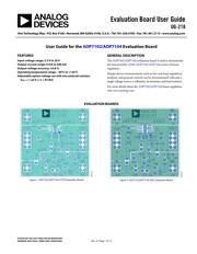
User Guide for the ADP7102/ADP7104 Evaluation Board
PLEASE SEE THE LAST PAGE FOR AN IMPORTANT
WARNING AND LEGAL TERMS AND CONDITIONS.
Rev. A | Page 1 of 12
FEATURES
Input voltage range: 3.3 V to 20 V
Output current range: 0 mA to 500 mA
Output voltage accuracy: ±0.8 %
Operating temperature range: −40°C to +125°C
Adjustable option voltage set with two external resistors
V
OUT
= 1.22 V × (1 + R1/R2)
GENERAL DESCRIPTION
The ADP7102/ADP7104 evaluation board is used to demonstrate
the functionality of the ADP7102/ADP7104 series of linear
regulators.
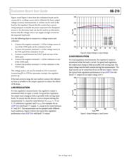
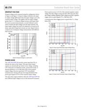
Simple device measurements such as line and load regulation,
dropout, and ground current can be demonstrated with just a
single voltage source, a voltmeter, an ammeter, and load resistors.
For more details about the ADP7102/ADP7104 linear regulators,
visit www.analog.com.
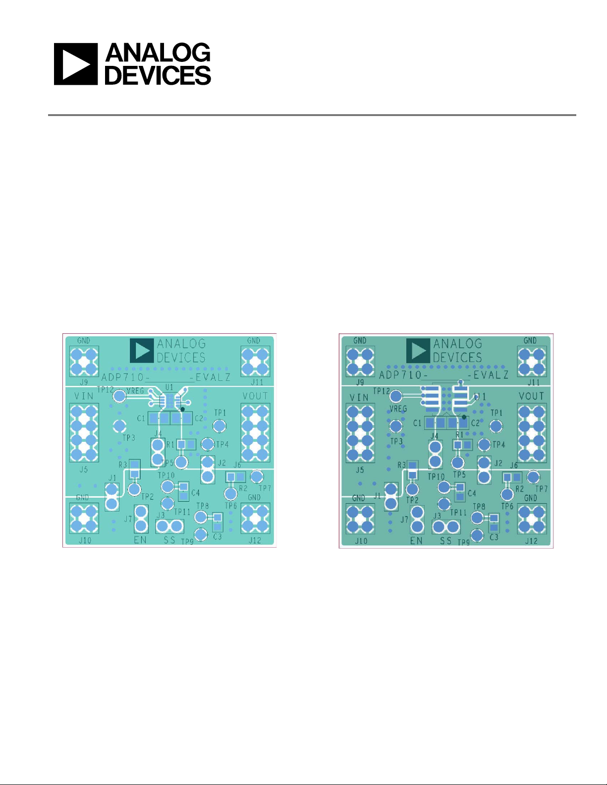
EVALUATION BOARDS
09509-001
Figure 1. ADP7102/ADP7104 LFCSP Evaluation Board
09509-002
Figure 2. ADP7102/ADP7104 SOIC Evaluation Board