

下载
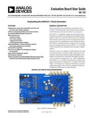
Evaluation Board User Guide
UG-182
One Technology Way • P. O. Box 9106 • Norwood, MA 02062-9106, U.S.A. • Te l: 781.329.4700 • Fax: 781.461.3113 • www.analog.com
Evaluating the AD9523-1 Clock Generator
PLEASE SEE THE LAST PAGE FOR AN IMPORTANT
WARNING AND LEGAL TERMS AND CONDITIONS.
Rev. 0 | Page 1 of 16
FEATURES
Simple power connection using USB connection and
on-board LDO voltage regulators
LDOs are easily bypassed for power measurements
AC-coupled differential SMA connectors
SMA connectors for
2 reference inputs
2 PLL status outputs
1 reference test input
2 VCXO interface inputs/outputs
Microsoft Windows®–based evaluation software
with simple graphical user interface
On-board PLL loop filter
Easy access to digital I/O and diagnostic signals
via I/O header
Status LEDs for diagnostic signals
USB computer interface
Software calculator provides flexibility, allowing programming
of almost any rational input/output frequency ratio
GENERAL DESCRIPTION
This user guide describes the hardware and software of the
AD9523-1 evaluation boards. The evaluation board schematic
and PCB layout artwork can be found at www.analog.com.
The AD9523-1 is designed to support the clock requirements
for long-term evolution (LTE) and multicarrier GSM base station
designs. It relies on an external VCXO to provide the reference
jitter cleanup to achieve the restrictive low phase noise require-
ments necessary for acceptable data converter SNR performance.
The AD9523-1 evaluation board is a compact, easy-to-use plat-
form for evaluating all features of the AD9523-1. A 122.88 MHz
VCXO is mounted on the evaluation board to provide a complete
solution.
The input receivers are configured as differential but the evalua-
tion board has baluns to provide a single-ended input for easy
evaluation using common laboratory single-ended signal sources.
Output 8 is connected to an ADCLK905 clock buffer to provide
a way to evaluate an Analog Devices, Inc., buffer. Although the
ADCLK905 is a 1-to-1 buffer, the performance is similar to the
larger fanout buffer, for example, the 1-to-2 buffer, ADCLK925.
Output 1 and Output 9 are configured with baluns to provide a
single-ended output to drive most test equipment. Output 0 is
configured for differential zero delay operation.
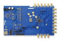
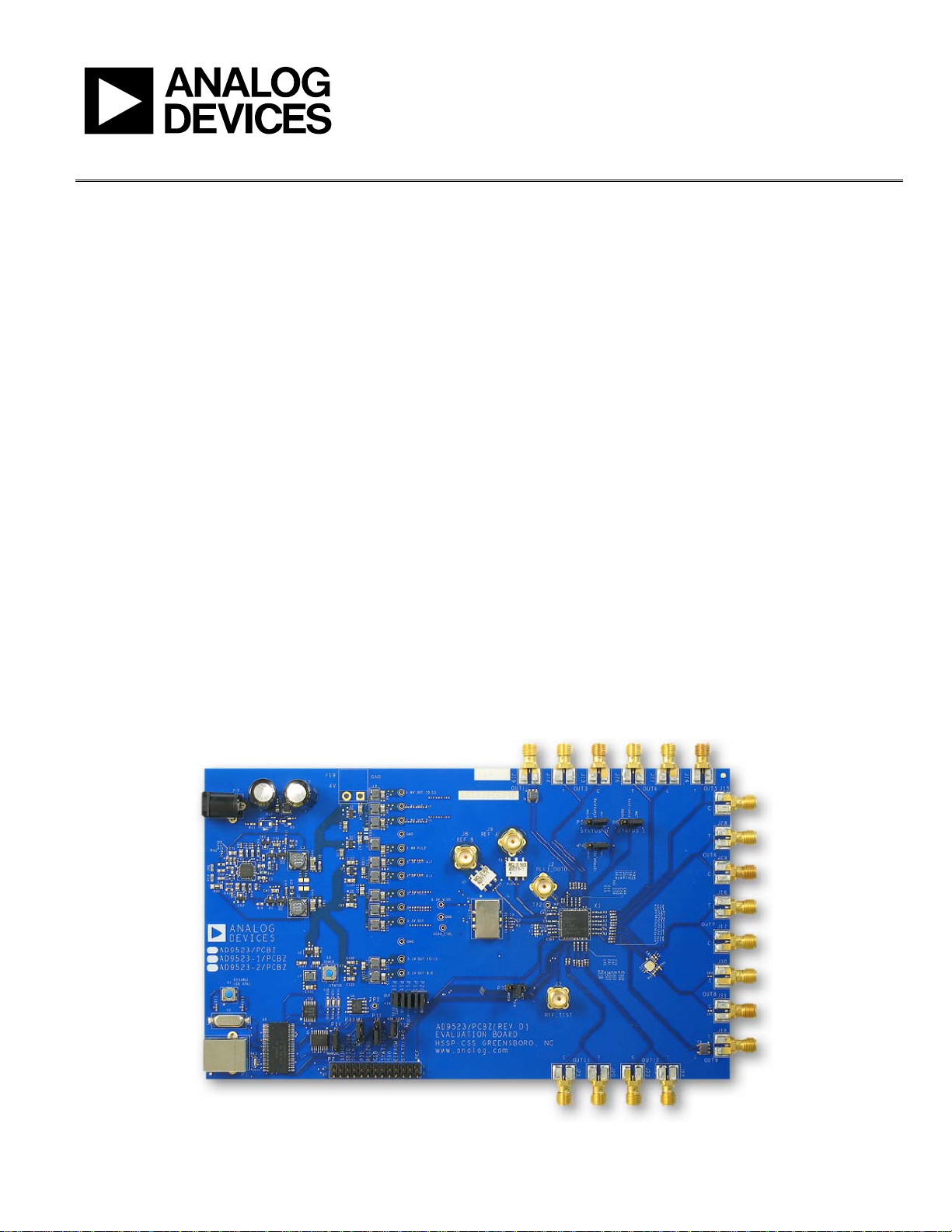
DIGITAL PICTURE OF EVALUATION BOARD
09280-001
Figure 1.
AD9523-1 Evaluation Board