


下载
Multiple Output, High Precision,
Dual-Tracking Reference
Data Sheet
AD588
Rev. M Document Feedback
Information furnished by Analog Devices is believed to be accurate and reliable. However, no
responsibility is assumed by Analog Devices for its use, nor for any infringements of patents or other
rights of third parties that may result from its use. Specifications subject to change without notice. No
license is granted by implication or otherwise under any patent or patent rights of Analog Devices.
Trademarks and registered trademarks are the property of their respective owners.
One Technology Way, P.O. Box 9106, Norwood, MA 02062-9106, U.S.A.
Tel: 781.329.4700 ©1986–2015 Analog Devices, Inc. All rights reserved.
Technical Support www.analog.com
FEATURES
Low drift: 1.5 ppm/°C
Low initial error: 1 mV
Pin programmable output
+10 V, +5 V, ±5 V tracking, −5 V, −10 V
Flexible output force and sense terminals
High impedance ground sense
16-lead SOIC package and 16-lead CERDIP
MIL-STD-883-compliant versions available
GENERAL DESCRIPTION
The AD588 represents a major advance in state-of-the-art
monolithic voltage references. Low initial error and low
temperature drift give the AD588 absolute accuracy performance
previously not available in monolithic form. The AD588 uses a
proprietary ion-implanted, buried Zener diode and laser-wafer
drift trimming of high stability thin film resistors to provide
outstanding performance.
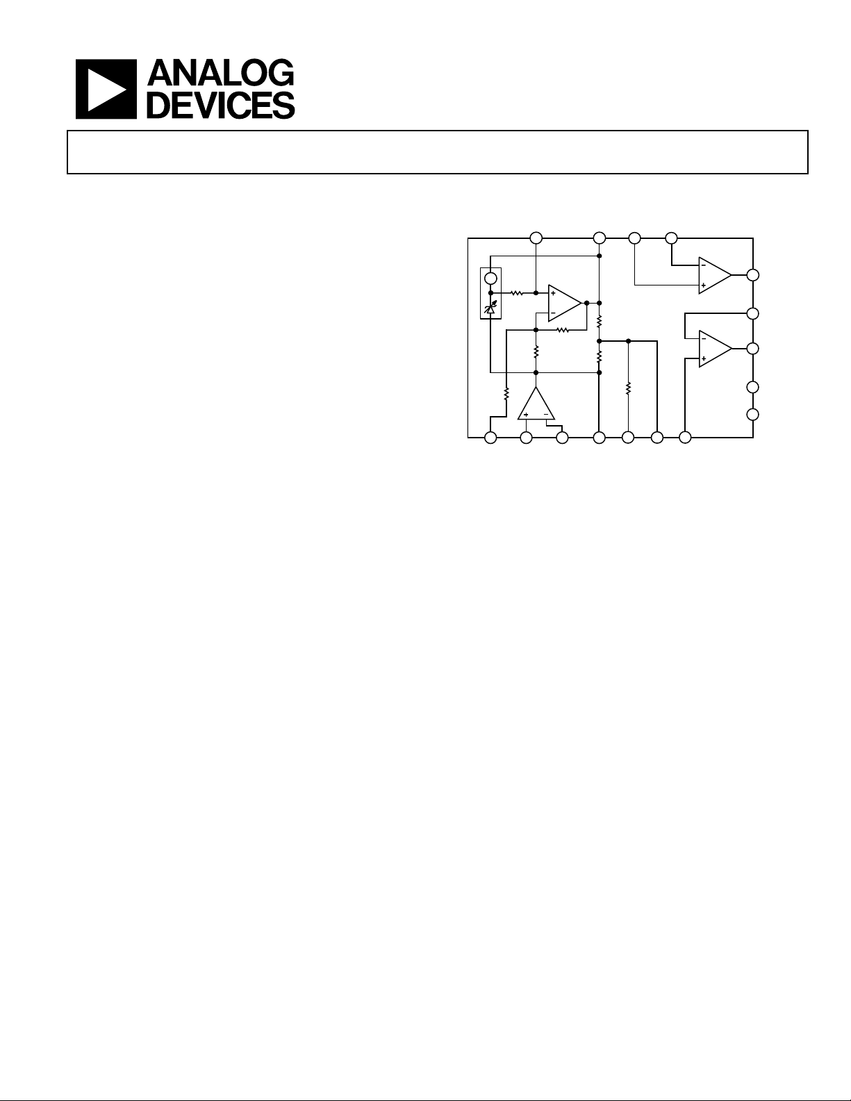
The AD588 includes the basic reference cell and three additional
amplifiers that provide pin programmable output ranges. The
amplifiers are laser trimmed for low offset and low drift to maintain
the accuracy of the reference. The amplifiers are configured to
allow Kelvin connections to the load and/or boosters for driving
long lines or high current loads, delivering the full accuracy of
the AD588 where it is required in the application circuit.
The low initial error allows the AD588 to be used as a system
reference in precision measurement applications requiring
12-bit absolute accuracy. In such systems, the AD588 can provide a
known voltage for system calibration in software. The low drift
also allows compensation for the drift of other components in a
system. Manual system calibration and the cost of periodic
recalibration can, therefore, be eliminated. Furthermore, the
mechanical instability of a trimming potentiometer and the
potential for improper calibration can be eliminated by using
the AD588 in conjunction with auto calibration software.
The AD588 is available in seven versions. The AD588JQ and
AD588KQ are packaged in a 16-lead CERDIP and are specified
for 0°C to +70°C operation. The AD588AQ and AD588BQ are
packaged in a 16-lead CERDIP, and the AD588ARWZ is packaged
in a 16-lead SOIC, and they are specified for the −25°C to +85°C
industrial temperature range. The ceramic AD588TE and
AD588TQ grades are specified for the full military/aerospace
temperature range.
FUNCTIONAL BLOCK DIAGRAM
R3
R
B
R1
R2
R4
R5
R6
GAIN
ADJ
GND
SENSE
+IN
GND
SENSE
–IN
V
LOW
BAL
ADJ
V
CT
A4 IN
–V
S
+V
S
A4 OUT
FORCE
A4 OUT
SENSE
A3 OUT
FORCE
A3 OUT
SENSE
A3 IN
V
HIGH
NOISE
REDUCTION
A1
A4
AD588
00531-001
A3
13
11
12
8
10
95
1
14
15
2
16
34
6
7
A2
Figure 1.
PRODUCT HIGHLIGHTS
1. The AD588 offers 12-bit absolute accuracy without any
user adjustments. Optional fine-trim connections are
provided for applications requiring higher precision. The
fine trimming does not alter the operating conditions of
the Zener or the buffer amplifiers, and so does not increase
the temperature drift.
2. Output noise of the AD588 is very low, typically 6 µV p-p.
A pin is provided for additional noise filtering using an
external capacitor.
3. A precision ±5 V tracking mode with Kelvin output
connections is available with no external components.
Tracking error is less than 1 mV, and a fine trim is available
for applications requiring exact symmetry between the
+5 V and −5 V outputs.
4. Pin strapping capability allows configuration of a wide
variety of outputs: ±5 V, +5 V, +10 V, −5 V, and −10 V dual
outputs or +5 V, −5 V, +10 V, and −10 V single outputs.
页面指南