
下载
Semiconductor Components Industries, LLC, 2011
December, 2011 − Rev. 10
1 Publication Order Number:
UMC2NT1/D
UMC2NT1G,
NSVUMC2NT1G,
UMC3NT1G,
NSVUMC3NT1G,
UMC5NT1G,
NSVUMC5NT2G
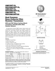
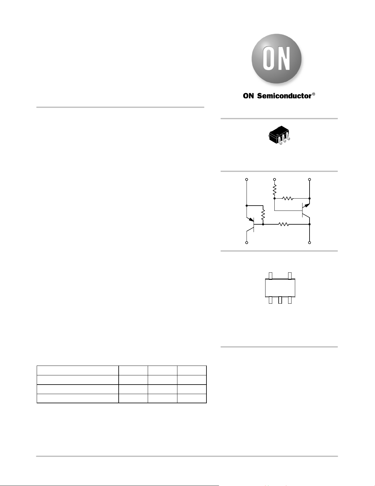
Dual Common
Base-Collector Bias
Resistor Transistors
NPN and PNP Silicon Surface Mount
Transistors with Monolithic Bias
Resistor Network
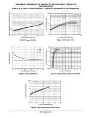
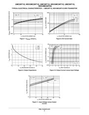
The Bias Resistor Transistor (BRT) contains a single transistor with
a monolithic bias network consisting of two resistors; a series base
resistor and a base−emitter resistor. These digital transistors are
designed to replace a single device and its external resistor bias
network. The BRT eliminates these individual components by
integrating them into a single device. In the UMC2NT1G series, two
complementary BRT devices are housed in the SOT−353 package
which is ideal for low power surface mount applications where board
space is at a premium.
Features
Simplifies Circuit Design
Reduces Board Space
Reduces Component Count
Available in 8 mm, 7 inch/3000 Unit Tape and Reel
AEC−Q101 Qualified and PPAP Capable
NSV Prefix for Automotive and Other Applications Requiring
Unique Site and Control Change Requirements
These Devices are Pb−Free, Halogen Free/BFR Free and are RoHS
Compliant*
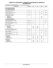
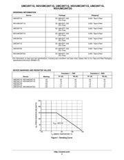
MAXIMUM RATINGS (T
A
= 25C unless otherwise noted, common for
Q
1
and Q
2
, − minus sign for Q
1
(PNP) omitted)
Rating
Symbol Value Unit
Collector-Base Voltage V
CBO
50 Vdc
Collector-Emitter Voltage V
CEO
50 Vdc
Collector Current I
C
100 mAdc
Stresses exceeding Maximum Ratings may damage the device. Maximum
Ratings are stress ratings only. Functional operation above the Recommended
Operating Conditions is not implied. Extended exposure to stresses above the
Recommended Operating Conditions may affect device reliability.
*For additional information on our Pb−Free strategy and soldering details, please
download the ON Semiconductor Soldering and Mounting Techniques
Reference Manual, SOLDERRM/D.
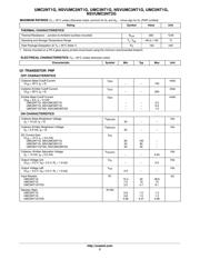
SC−88A/SOT−353
CASE 419A
STYLE 6
Ux = Device Marking
x = 2, 3 or 5
M = Date Code
G = Pb−Free Package
MARKING DIAGRAM
132
54
45
Q1
Q2
R1
R1
R2
R2
312
See detailed ordering and shipping information in the package
dimensions section on page 4 of this data sheet.
ORDERING INFORMATION
http://onsemi.com
Ux M G
G
(Note: Microdot may be in either location)
页面指南