

下载

Application Report
SLUA709 – March 2014
1
UCD3138 PFC Tuning
Bosheng Sun, Zhong Ye High Performance Isolated
ABSTRACT
PFC current loop tuning is a time consuming and challenging task for the PFC design engineer. It
requires the current waveform not only to be stable, but also to be smooth with very low total harmonic
distortion (THD) and high power factor (PF). It gets more and more challenging with the ever increasing
THD and PF requirements. Although digital controller provides more flexibility and better performance,
loop tuning still requires significant effort, especially for the engineers new to PFC design, the word
“digital” may also sounds scary for people switching from analog control to a digital solution. This
application note provides a step by step guide of how to tune the current loop of a UCD3138 [1]
controlled PFC, as well as some techniques to reduce THD and improve PF.
Contents
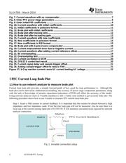
1 PFC Current Loop Bode Plot .............................................................................................................. 2
1.1 How to use network analyzer to measure bode plot ............................................................... 2
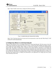
1.2 Voltage loop effects on current loop bode plot ....................................................................... 3
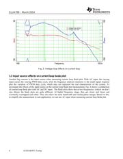
1.3 Input source effects on current loop bode plot ........................................................................ 4
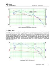
1.4 CCM vs. DCM ......................................................................................................................... 5
2 UCD3138 Digital Compensator ........................................................................................................... 6
3 Tuning a PFC Current Loop................................................................................................................ 6
3.1 Get initial compensator coefficients ........................................................................................ 6
3.2 Tuning 1-pole 1-zero compensator ....................................................................................... 10
3.3 Tuning 2-pole 2-zero compensator ....................................................................................... 15
4 Adding Current Reference Offset .................................................................................................... 16
5 Dynamic Loop Compensation .......................................................................................................... 18
6 Oversampling .................................................................................................................................... 18
7 Current Distortion Reduction at DCM Mode ................................................................................... 19
8 Adding Sample Trigger Offset .......................................................................................................... 20
9 Harmonic Injection ............................................................................................................................ 21
10 EMI Filter X-CAP Reactive Current Compensation ...................................................................... 21
11 Reduce the Voltage Loop Effect .................................................................................................... 22
Reference .............................................................................................................................................. 22
Figures
Fig. 1. Venable connection setup.......................................................................................................... 2
Fig. 2. Venable bode plot measurement setting .................................................................................. 3
Fig. 3. Voltage loop effects on current loop ......................................................................................... 4
Fig. 4. Input source effects on current loop ......................................................................................... 5
Fig. 5. Bode plot at CCM vs. DCM ......................................................................................................... 5
Fig. 6. UCD3138 PID structure ............................................................................................................... 6