
下载
DN-97
Design Note
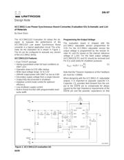
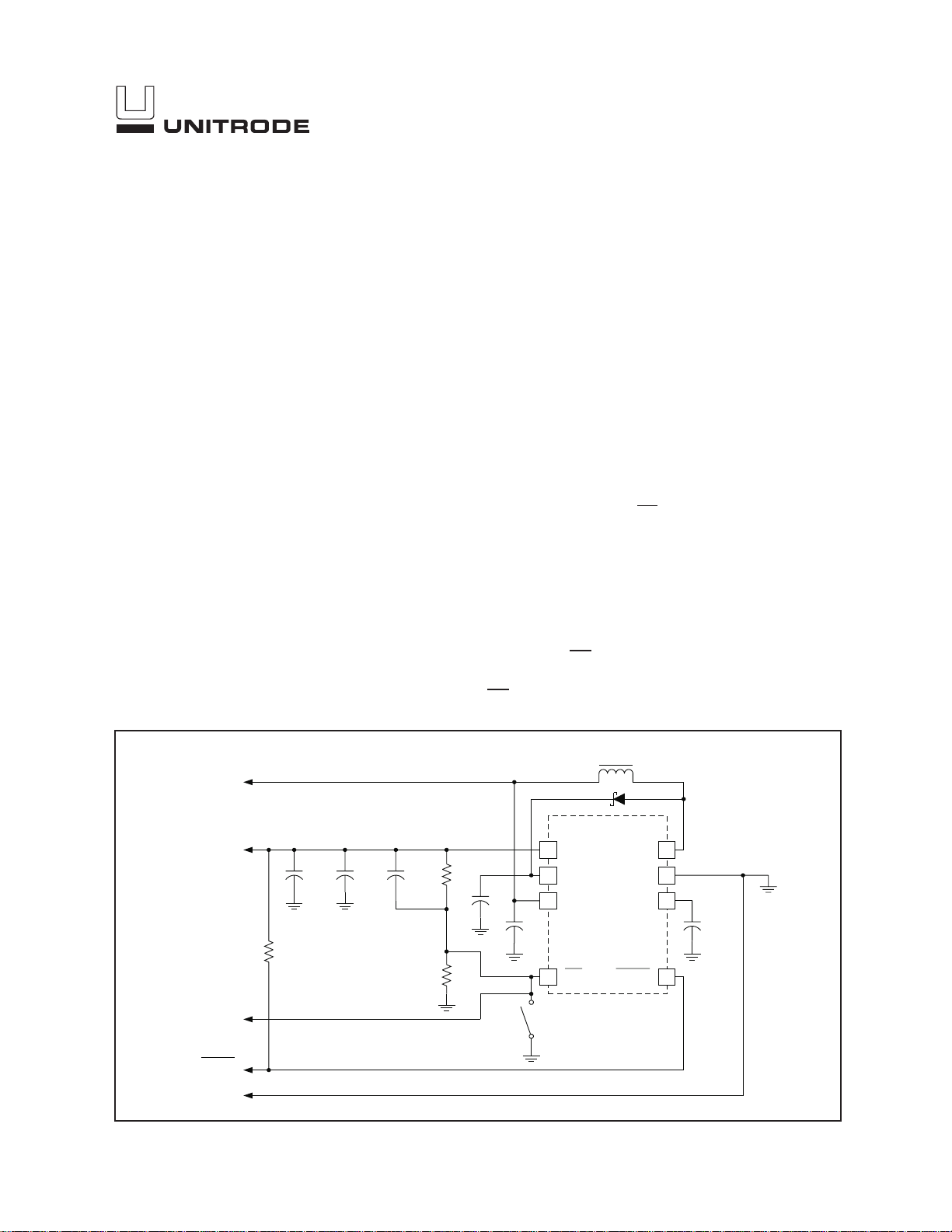
The UCC39411/2/3 Evaluation Kit allows the de-
signer to evaluate the performance of the
UCC39411/2/3 Low power Synchronous Boost
converter in a typical application circuit. The sche-
matic for the evaluation kit is shown in Figure 1.
The kit can be configured to evaluate any version
of the UCC39411 family.
UCC39411/2/3 Features
•
8 pin TSSOP package
•
startup guaranteed under full load conditions at
VBAT ≥ 1V
•
Operation down to 0.5V after startup
•
Wide input voltage range: 1V to 3.2V
• 200mW output power with VBAT as low as 0.8V
• Secondary supply voltage from a single inductor
• Output fully disconnected in shutdown
•
Adaptive current mode control for optimum
efficiency
•
Low shutdown supply current
•
Built-in Reset function with programmable reset
pulse width
Programming the Output Voltage
The evaluation board is shipped with the
UCC39411 adjustable version programmed for
3.3V. For the UCC39411 adjustable version the
output voltage is programmed by the resistor di-
vider R1 and R2 based on the internal reference
voltage of 1.25V. For the fixed output voltages
(UCC39412/3) R1 and R2 should be removed and
Pin 4 is used solely for shutdown purposes.
V
R
R
OUT
=•+
125 1
1
2
.
(1)
Note that the Thevenin impedance at the Feedback
pin must be > 200kΩ.
When designing with the UCC39411 IC (adjustable
output), it is important to populate capacitor C5.
Capacitor, C5, provides feed forward from the out-
put to the SD
/FB pin to compensate for delays
caused by the high impedance requirements of the
SD
/FB pin and the parasitic capacitance on that
04/99
UCC39411 Low Power Synchronous Boost Converter, Evaluation Kit, Schematic and List
of Materials
By Dave Olson
7
1
8
2
VOUT
6
4
5
3
SW
VGD GND
VBAT
CT
SD/FB RESET
UCC39411
L1
22µF
D1
C3
10µF
+
C4
0.047µF
C2
10µF
+
R1
768k
R2
464k
C5
120pF
PROV
C1
100µF
+
R3
10k
SW1
VBAT
P1
VOUT
P3
SHUTDOWN
P4
RESET
P5
GND
P2
C6
0.01µF
Figure 1. UCC39411/2/3 evaluation kit.
UDG-99049