
下载
Application Report
SLVA744–January 2016
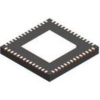
Build a High-Density, High Refresh Rate, Multiplexing
Panel With the TLC59581
Ge,Rosley
ABSTRACT
The application note describes the detailed steps to build a high-density, high refresh rate, multiplexing
panel with the TLC59581. Detailed configurations and system structure guidelines are included in this
report.
Contents
1 Introduction ................................................................................................................... 2
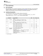
2 Device Specification......................................................................................................... 5
2.1 Basic Information ................................................................................................... 5
2.2 Switching Characteristics.......................................................................................... 5
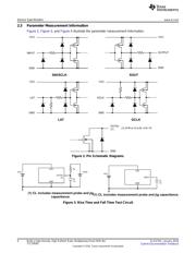
2.3 Parameter Measurement Information ............................................................................ 6
2.4 Timing Diagrams.................................................................................................... 7
3 Detailed Description......................................................................................................... 8
3.1 How to use the TLC59581......................................................................................... 8
3.2 Step 1 — Choose BC and CC, Select R
IREF
..................................................................... 8
3.3 Step 2 — Write Function Control Register FC1 and FC2.................................................... 11
3.4 Step 3 — Write GS Data Into One Memory BANK ........................................................... 18
3.5 Step 4 — Send Vsync Command to Switch the BANK Purpose............................................ 23
3.6 Step 5 — Input GCLK to Begin Displaying the Image of One New Frame................................ 23
3.7 Step 6 — During the Same Period of Step 5, Write GS Data for Next Frame Into Another BANK .... 28
3.8 Step 7 — When the Time of One Frame Ends, Input the Vsync Command to Swap the Purpose
of the Two BANKs ................................................................................................ 28
3.9 LED Open Detection (LOD)...................................................................................... 29
3.10 How to Read the Function Control Register................................................................... 33
3.11 Function Commands Summary ................................................................................. 34
3.12 Power-Save Mode (PSM) ........................................................................................ 35
3.13 Pre-Charge Function.............................................................................................. 36
3.14 1
st
-Line Enhancement............................................................................................. 38
3.15 HG-LG Interference Enhancement.............................................................................. 38
3.16 Low Gray-Scale Enhancement.................................................................................. 39
3.17 LOD Caterpillar Cancelling....................................................................................... 40
3.18 Protection........................................................................................................... 41
3.19 System Structure Guidelines .................................................................................... 41
List of Figures
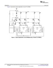
1 Typical Application Circuit (Multiple Daisy Chained TLC59581s) ..................................................... 4
2 Pin Schematic Diagrams.................................................................................................... 6
3 Rise Time and Fall Time Test Circuit ..................................................................................... 6
4 Constant Current Test Circuit for OUTXn ................................................................................ 7
5 Output Timing ................................................................................................................ 7
6 Common Shift Register and Data Latch Configuration................................................................ 11
All trademarks are the property of their respective owners.
1
SLVA744–January 2016 Build a High-Density, High Refresh Rate, Multiplexing Panel With the
TLC59581
Submit Documentation Feedback
Copyright © 2016, Texas Instruments Incorporated