


下载
APPLICATION NOTE
TD310 USED IN A HIGH SIDE DRIVING
AN853/0299
by R. LIOU
®
The TD310 is a triple MOS or IGBT driver which
integrates all functions suited for compact and
highly secure driving such as adjustable Under
Voltage Lockout feature (UVLO), sense compara-
tor with alarm output and automatic shutdown,
independent operational amplifier, enable pin, and
global standby mode (e.g.: for portable applica-
tions).
Its wide operating supply voltage range makes it
appropriate in many different applications, in par-
ticular in 12V supplied automotive field.
The following shows how secure high side driving
is easily achievable using few external and low cost
components in very common lamp high side driving
applications.
PRINCIPLE
The Op Amp is used as an oscillator by means of
the R1C1 backloop (blinker frequency ~1Hz) and
enables/disables the charge pump that drives the
high side MOS Q1.
The charge pump is made using one of the three
inverting buffers mounted as an oscillator with the
R2C2 backloop (charge pump frequency
~100kHz). The capacitor C is used to transfer the
buffer high state voltage to the gate of Q1.
The diode D1 refrains the gate from discharging
and the diode D2 shifts the voltage across C above
the source of Q1.
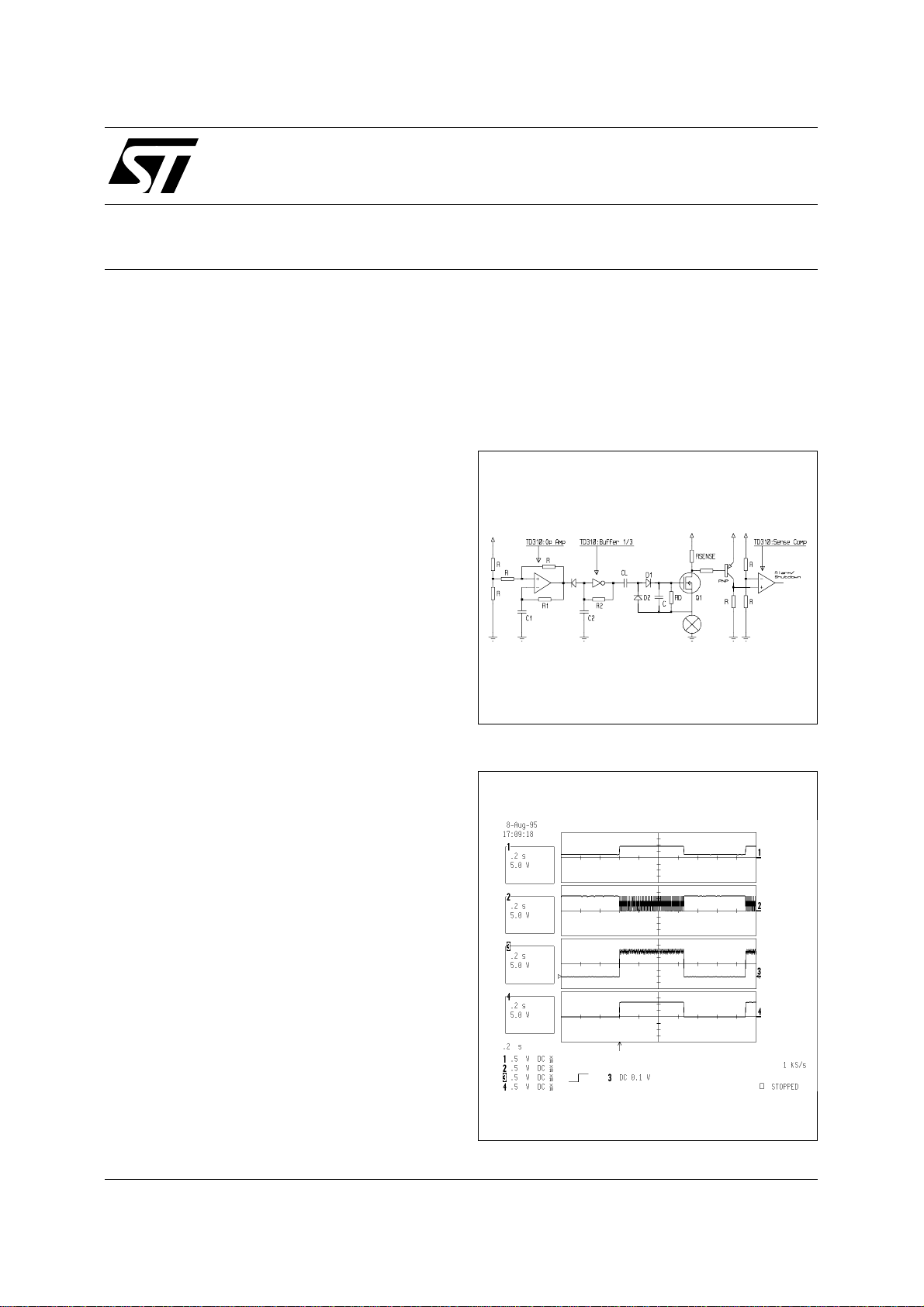
Figure 1 shows the blinker application schematic,
and figures 2 and 3 show the resulting traces:
.trace 1 : the Op Amp output
.trace 2 : the inverting buffer output
.trace 3 : the transistor Q1 gate (low Ron)
.trace 4 : the load (12V/21W lamp)
INTRODUCTION
Figure 1
Figure 2
1/3